| Posted: May 12, 2017 |
A novel method for the synthesis of hexagonal boron nitride
(Nanowerk News) A team of researchers from the Air Force Research Laboratory, Colorado School of Mines, and the Argonne National Laboratory in Illinois have developed a novel method for the synthesis of a composite material that has the potential of vastly improving the electronics used by the Air Force.
|
|
The material, hexagonal boron nitride (hBN), is similar to graphene and can be formed and stabilized to a layered thickness of one atom. This synthesis of hBN in a controlled layer-by-layer fashion is critical to a number of applications, including tunneling barriers, used in transistors for low power devices, atomically thin capacitors, and two-dimensional (2D) transistors, which are smaller and use much less power than traditional silicon transistors.
|
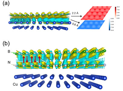 |
| A graphical representation of hexagonal boron nitride (hBN) grown on metal. (U.S. Air Force image)
|
|
“Fabricating devices from atomically thin 2D layers represents the future of nano-electronics,” states Dr. Michael Snure, AFRL senior research physicist. “This development significantly increases device density, improving flexibility and significantly reducing power requirements.”
|
|
As a 2D material, hBN has been of international interest for close to a decade. Researchers with AFRL’s Sensors Directorate have been working on experimental methods for developing this technology since 2013, with Dr. Snure leading the effort. Dr. Stefan Badescu, AFRL research physicist, joined the team in 2015 to lead the computational modeling research that has assisted the team with understanding the system’s properties and the mechanism for growth.
|
|
So how is a composite material intended for use in electronics scaled down to the thickness of a mere atom? Through a novel and complex method of synthesis, of course. Using a process that involves metal-organic chemical vapor disposition, the team discovered how to control the growth of hBN layers on a nanoscale.
|
|
The hBN from AFRL’s work is currently being used in the development of prototype 2D electronics devices including transistors and photodetectors. However, the impact of this development reaches further.
|
|
“By developing a model of growth, our work more broadly benefits the field of materials science in the areas of thin film growth and chemical vapor disposition,” reflects Badescu. “This modeling will help drive new discoveries in the synthesis of 2D materials.”
|
|
Badescu adds that future applications of hBN include transistors for switching and logic devices that are flexible, transparent, low power, and high frequency. The next steps are to demonstrate the feasibility of integrating hBN with other 2D semiconductors, including graphene and phosphorene.
|
|
The team’s work was published in a paper by Nano Letters ("Heterogeneous Pyrolysis: A Route for Epitaxial Growth of hBN Atomic Layers on Copper Using Separate Boron and Nitrogen Precursors"), and the team is considering filing a patent for the technology and synthesis method pending successful future experiments with hBN and metal combinations.
|