| Posted: May 30, 2017 |
Seeing below the surface of solar cells
(Nanowerk News) It’s difficult to improve processes you can’t see. That’s the problem for solar cells made of super-thin films. These highly flexible cells aren’t as efficient as they could be at converting sunlight to electricity.
|
|
A team of Molecular Foundry scientists and industry users developed a way to “see inside” thin-film solar cells. They can see the subsurface realm—where much of the energy-conversion action happens (Advanced Materials, "3D lifetime tomography reveals how CdCl2 improves recombination throughout CdTe solar cells").
|
|
This imaging technique lets them map the cells in three dimensions during operation as they absorb sunlight.
|
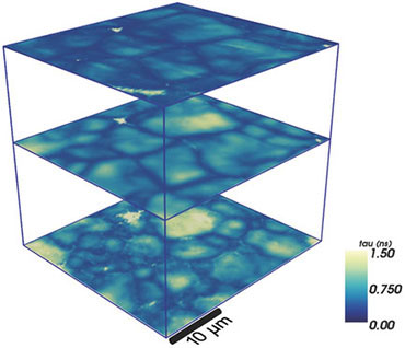 |
| A 3-D rendering of a thin-film cadmium telluride solar cell. The newly developed imaging technique shows how a solar cell’s surface and bulk “light up” (yellow) when a cadmium telluride solar cell is working (darker blue regions indicate no activity).Light penetrating from the top into the solar cell is converted to electricity more efficiently in the yellow regions of the device. (Image: Molecular Foundry, Berkeley Lab)
|
|
This unique tool will enable the solar industry to more rapidly develop reproducible high-efficiency solar cells. The tool provides a 3-D map of how photons interact with the material to make electricity to identify obstacles that dampen the efficiency of solar cells.
|
|
The tool offers images with a resolution at the micron scale, or approximately one hundredth the diameter of a human hair.
|
|
Next-generation solar cells made of super-thin films of semiconducting material hold promise because they’re relatively inexpensive and flexible. Dramatically increasing the efficiency of thin-film solar cells is a tough challenge, partly because a solar cell’s subsurface realm—where much of the energy-conversion action happens—is inaccessible to real-time, nondestructive imaging.
|
|
Scientists from the Molecular Foundry have developed a way to use optical microscopy to map—with micron resolution—thin-film solar cells in three dimensions as the cells absorb photons.
|
|
The method uses a highly focused laser beam of infrared photons that penetrates inside the photovoltaic material. When two low-energy photons converge at the same pinpoint, there’s enough energy to excite electrons. These electrons can be tracked to see how long they last in their excited state and the obstacles they encounter, including grain boundaries and substrate interfaces. Long-lifetime electrons appear as bright spots in microscopy images.
|
|
In a solar cell, long-lifetime electrons are more likely to result in electrical current. In addition, the imaging tool can create a 3-D map of a solar cell’s entire optoelectronic dynamics.
|
|
So far, scientists have used the technique to better understand why adding a specific chemical to solar cells made of cadmium telluride—the most common thin-film material—improves the solar cells’ performance.
|