| Posted: Jun 13, 2017 |
Amazing spintronics
(Nanowerk News) An electron carries electrical charge and spin that gives rise to a magnetic moment and can therefore interact with external magnetic fields. Conventional electronics are based on the charge of the electron. The emerging field of spintronics aims to exploit the spin of the electron. Using spins as elementary units in computing and highly efficient electronics is the ultimate goal of spintronic science because of spintronics minimal energy use.
|
|
In this study (Physical Review Letters, "Enhancement of thermally injected spin current through an antiferromagnetic insulator"), researchers manipulated and amplified the spin current through the design of the layered structures, a vital step towards this goal.
|
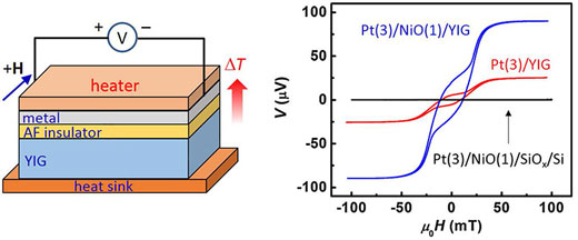 |
| Devices that take advantage of spin currents for their special electronic properties are made up of multiple layers of materials. For the measurements in this research, a device was made up of yttrium iron garnet (YIG) and a normal metal separated by an antiferromagnetic (AF – a material whose magnetic moments are canceled) insulating layer. (The heat sink and heater allowed a temperature gradient (T) for the spin current generation). The introduction of the AF insulating layer amplifies the spin current (blue curve in right figure) as compared to the plain metal-YIG interface (red curve) by up to a factor of 10. In the absence of the ferromagnetic YIG substrate, the spin current disappears (black line). The data in the figure was for a platinum (Pt) metal layer; the data correlate the applied field (H) with the measured inverse spin Hall voltage (V). (Image: C.L. Chien and the American Physical Society; modified by Claire Ballweg, Department of Energy)
|
|
For cell phones, computers, and other electronic devices, a major shortcoming is the generation of heat when electrons move around the electronic circuits. The energy loss significantly reduces the device efficiency. Ultimately, the heat limits the packing of components in high-density micro-chips.
|
|
Spintronics’ promise is to eliminate this energy loss. It does so by just moving the electron spin without moving the electrons. Using design strategies such as those identified by this research could result in highly energy-efficient spintronics to replace today’s electronics.
|
|
An important obstacle to realizing spintronics is the amplification of small spin signals. In conventional electronics, amplification of an electron current is achieved using transistors.
|
|
Recently, researchers at Johns Hopkins University demonstrated that small spin currents can be amplified by inserting thin films of antiferromagnetic (materials in which the magnetic moments are canceled ) insulator materials into the layered structures, effectively producing a spin-transistor.
|
|
Scientists used thin films of antiferromagnetic insulators, such as nickel and cobalt oxide, sandwiched between ferrimagnetic insulator yttrium iron garnet (YIG) and normal metal films. With such devices, they showed that the pure spin current thermally injected from YIG into the metal can be amplified up to ten-fold by the antiferromagnetic insulator film.
|
|
The researchers found that spin fluctuation of the antiferromagnetic insulating layer enhances the spin current. They also found that the amplification is linearly proportional to spin mixing conductance of the normal metal and the YIG.
|
|
The experiments demonstrated this effect for various metals. Further, the study showed that the spin current amplification is proportional to the spin mixing conductance of YIG/metal systems for different metals. Calculations of the spin current enhancement and spin mixing conductance provided qualitative agreement with the experimental observations.
|