| Posted: Jun 15, 2017 |
Seeking out new functions for superconducting nanoelectronics
(Nanowerk News) A team of researchers at the University of Tokyo and their collaborators discovered that a two-dimensional semiconductor with a broken inversion symmetry demonstrates rectification, or the property of a diode, under a magnetic field applied in a certain direction (Science Advances, "Nonreciprocal charge transport in noncentrosymmetric superconductors"). This finding provides important insights essential for developing the next generation of superconducting nanoelectronics materials.
|
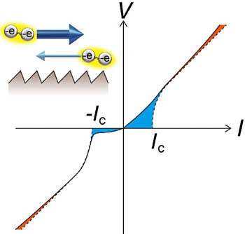 |
| Rectification property in the superconducting state. In general, a magnetic field applied in a specific direction in a system in which the spatial inversion symmetry is broken generates rectifying characteristics, but the rectification property is larger in the superconducting state, compared to the normal conducting state. (Image: Ryohei Wakatsuki, Yu Saito)
|
|
Superconductivity is a property in which electrical resistance disappears; it has been the focus of much basic and applied research around the world as a next-generation technology that could enhance energy conservation.
|
|
The integration of superconductors is expected to play an important role in next-generation computing systems, such as in the area of superconducting quantum bits; thus, there is much demand for the development of new functions of superconducting nanoelectronics for these purposes—especially superconductors with a rectifying property, i.e., superconducting diodes.
|
|
Although recent research has revealed rectification in a normal conductor crystal with a broken inversion symmetry, not much research has been conducted on the rectification property of a superconductor lacking inversion symmetry.
|
|
The research group led by graduate students Ryohei Wakatsuki and Yu Saito, Professor Yoshihiro Iwasa, and Professor Naoto Nagaosa at the Graduate School of Engineering, the University of Tokyo, and their collaborators fabricated an electric double-layer transistor (EDLT) structure, a kind of field effect transistor, using a high-quality single crystal of molybdenum disulfide (MoS2), a layered material that is a type of atomic film material.
|
|
The capacity of electrons induced by the strong electric field to accumulate on the surface of a single crystal of MoS2 in this structure makes it possible to realize synthetically the extremely thin, one-atomic-layer-thick ultimate two-dimensional superconductivity.
|
|
In the current study, the researchers measured the electric conduction characteristics of a MoS2-EDLT device with a magnetic field applied perpendicular to the surface. They observed extremely large rectifying characteristics in the superconducting state by measuring the second harmonic component of electric resistance to examine rectification.
|
|
Moreover, the scientists applied theoretical calculations for superconducting fluctuation currents to explain the mechanism of the enhanced rectification property, and showed that the phenomenon could occur in any superconductor with a broken inversion symmetry.
|
|
"The nonlinear response of rectifying characteristics and electric current discovered in this research is considered to be a universal phenomenon in superconductors in which the spatial inversion symmetry has been broken," says Professor Nagaosa. He continues, "The present result will pave the way for the development of functions of superconducting nanoelectronics, as well as become the cornerstone of a new academic field created to study two-dimensional superconductivity with broken spatial inversion symmetry."
|