| Posted: Aug 03, 2017 |
Using angles to improve the future of electronics
(Nanowerk News) While there is much hype around graphene, it’s considered to be one of the most promising materials for future semiconductor electronic and quantum devices due to its superior electronic properties. It also exhibits rich physical properties depending on how it is stacked on top of another 2D crystal, and here is where it gets really interesting and a little complicated.
|
|
When the two stacked layers are made of the same material, such as graphene, a special set of periodic 2D superlattices will emerge at specific angles. Such mismatch can also induce a bandgap in bilayer graphene systems producing one of the first steps towards building transistor-type devices for next generation electronic devices which are more powerful, yet energy efficient.
|
|
Koren and his colleagues published their initial results in the September 2016 issue of the peer-review journal Nature Nanotechnology ("Coherent commensurate electronic states at the interface between misoriented graphene layers"). In the paper the team demonstrated how by using the sharp-tip of an atomic force microscope they can precisely control what appears to look like a common house key (Fig.).
|
|
The nano-sized key-shaped device can be rotated like hands on a lock from 0 to 360 degrees, which could be used as a switch to turn on and off the current of a tunnel field effect transistor (TFET), an important step in reducing energy leakage in electronic devices.
|
|
“We have achieved unprecedented accuracy in controlling the rotational configuration with an angular resolution – better than 0.1 degrees. This enables us to both explore the fundamental nature of the stack and realize its full potential,” said Koren.
|
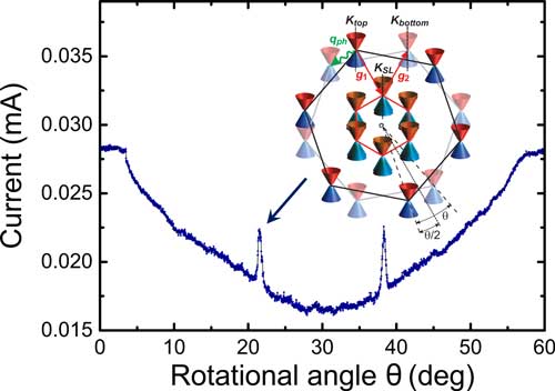 |
| Measured current flowing through the twisted graphite nanostructure at a bias potential of V= 50 mV while continuously rotating the lever arm. Inset: momentum-space representation of bilayer graphene coupling at commensurate twist angles θ=21.8° and 38.2°.
|
|
The ability to control the stacking configuration with high angular accuracy allows to control and engineer many physical properties and realize new novel materials in various fields in science and technology such as: electronics, optics, thermoelectrics and electromechanics.
|
|
The device also enables a high magnetic flux within a single crystal cell which produces the famous Hofstadter’s butterfly, the theorized behavior of electrons under a strong magnetic field and a periodic potential.
|
|
The laws of friction don’t escape the nano regime and even at this small scale friction becomes a challenge for the key-shaped device and as we know, friction causes heat, wear and dissipates energy — an unfortunate property at this scale.
|
|
Incredibly, the rotational mismatch in 2D layered systems strongly suppresses the friction and energy dissipation, an effect which is known as superlubricity.
|
|
“There is virtually no friction. It’s simply based on finding the right angle,” adds Koren.
|
|
Koren hopes that by sharing his research with others in the field it will spark some novel material and device designs.
|