| Posted: Aug 08, 2017 |
Beyond graphene: scientists are creating an atomic 'Lego set' of 2D wonder materials
(Nanowerk News) The strongest material known to mankind was first discovered with sticky tape. Today, this two-dimensional (2D) version of carbon known as graphene is the subject of intense research around the world. Many hope its unique properties could lead to breakthroughs in fields from electronics to medicine.
|
|
By 2D we mean it is made from a single layer of atoms. In graphene’s case, these are arranged in a hexagonal pattern that help make it incredibly strong. It also conducts electricity and heat at unprecedented levels, is impermeable to gases and can be both brittle and ductile.
|
|
Yet while graphene has received incredible attention and won its discoverers a Nobel Prize, it’s no longer alone in the world of 2D materials. Many other similar materials have since been predicted and isolated, each with similar structural properties to graphene but also a variety of unique individual characteristics.
|
|
In fact, there are so many 2D materials with such a wide variety of properties that we can effectively use them to design and build new 3D materials with the exact characteristics we want. This idea of an atomic-scale “Lego set” creates potentially infinite possibilities for new substances.
|
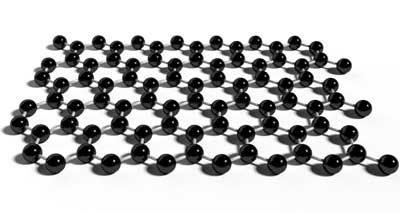 |
| Graphene, the original wonder material. (Image: Andrew Beckinsale)
|
|
Theoretically, almost any 3D material can have a 2D counterpart. The list so far includes: silicene (a single layer of silicon) ("Silicene, a promising new 2D material"), phosphorene (a single layer of black phosphorus) ("Phosphorene – The two-dimensional black phosphorous: Properties, synthesis and applications"), and various monolayers of chemical compounds known as transition-metal dichalcogenides (TMDCs) ("2D transition metal dichalcogenides"), such as molybdenum disulfide (MoS2) and molybdenum ditelluride (MoTe2).
|
|
Research is ongoing into probably dozens of methods to isolate these materials. The two main methods used are mechanical exfoliation – which was the method first used to make graphene by isolating individual layers with adhesive tape – and by effectively growing a 2D layer of crystals directly onto a flat base ("Metallic atomically-thin layered silicon epitaxially grown on silicene/ZrB2 ").
|
|
In practice, however, there are many limitations to what is currently possible. Only highly thermally and chemically stable materials can be separated into monolayers ("Van der Waals heterostructures"), which immediately discounts many elements. And, once isolated, many metallic monolayers in particular tend to corrode or oxidise in a way that destroys their desired properties.
|
|
Once you have a 2D material, you can then layer it with other substances of very different chemical properties to create “heterostructures”. For instance we can combine semiconductors with magnets, or metals with superconductors. The list of possible combinations grows exponentially.
|
|
These can be tailored with atomic precision using scanning tunnelling microscopes. These methods involve generating an electric current between a surface and the tip of the atomically fine probe to pick up and move individual atoms. One such 2D heterostructure that has been made in the lab combines atomic monolayers of graphene and hexagonal boron nitride (h-BN) ("Graphene, hexagonal boron nitride, and their heterostructures: properties and applications").
|
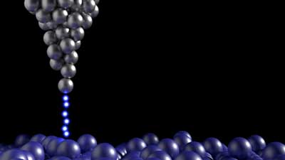 |
| Scanning tunnelling microscope. (Image: Andrew Beckinsale)
|
Completely new functionalities
|
|
Both 2D materials and heterostructures have already found many actual and potential applications across a broad range of areas. For example, graphene has made possible the dream of “printing” circuits onto flexible plastic bases ("Highly Flexible and Conductive Printed Graphene for Wireless Wearable Communications Applications"), at least in a lab. In the future, this could lead to consumer products such as flexible TVs, smartphones and more user-friendly wearable devices.
|
|
The discovery of a multitude of other 2D materials has opened up almost infinite ways of combining different properties, which could hugely improve or speed up the development of these applications. For example, using h-BN as the base for graphene electronics instead of the traditional silicon dioxide could mitigate some of the problems with the technology. Because h-BN monolayers are ultra-flat and can be isolated in the same way as graphene, it’s possible to remove atomic flaws in the base that interfere with the properties of the graphene sheet.
|
|
Furthermore, advancements in 2D materials research is enabling a new way of making computer processors even faster; something which is seen as vital to maintaining the progress of electronic technology. Computer chips make their calculations using large numbers of transistors, each of which works by moving electrons between different layers of semiconductor material.
|
|
Having more than one type of 2D material means you can use them to make each of the different semiconductor layers just one atom thick ("Two-dimensional materials: Atomically thin p–n junctions"). As transistors become smaller, more of them can be placed onto each computer chip, and this then naturally leads to the production of faster processors.
|
|
We could also see graphene and other 2D materials used to help generate and store energy. For example, graphene-based heterostructures can be used to help create highly efficient and flexible solar and fuel cells. These heterostructures are also being used to develop next-generation batteries and supercapacitors, which promise faster charging and extended energy output.
|
|
With the growth of electric cars and companies such as Tesla leading us towards a future of greener energy conversion and storage solutions, there is sure to be a huge focus on this sort of technology for the foreseeable future.
|