| Posted: Jun 01, 2017 | |
Metamaterial allows for ultraviolet nanolithography below the diffraction limit(Nanowerk News) Reporting their work in ACS Applied Materials & Interfaces ("Optically Patternable Metamaterial Below Diffraction Limit"), researchers in Korea report an optically patternable metamaterial comprised of monolayered silver nanoislands embedded within a photosensitive polymer resin for ultraviolet nanolithography. |
|
 |
|
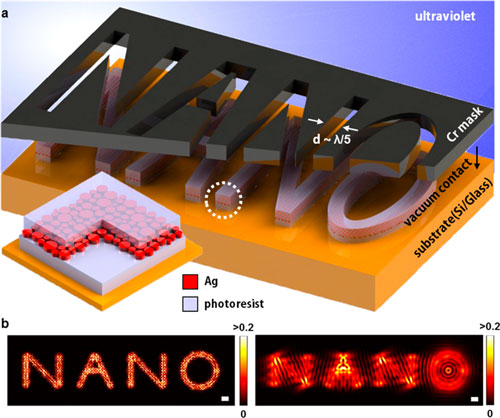
| (a) Schematic illustration of an optically patternable metamaterial (OPM) for ultraviolet nanolithography. The OPM consists of monolayered silver nanoislands sandwiched between two ultrathin photosensitive layers and exhibits the excitation of surface plasmons that preserves ultraviolet image patterns below the diffraction limit. After UV exposure, this unique configuration of embedded nanoislands facilitates the permeation of a developing solution, allowing it to rapidly pass through the top to the bottom of the OPM during the development process. (b) 2D E-field intensities of UV light (λ = 365 nm) on a silicon substrate propagating through the OPM (left) and through a conventional photoresist (right) of the same thickness, for a text Cr pattern of “NANO” with a 50 nm line width. The width, thickness, and gap of the islands are 20, 10, and 4 nm, respectively. Both of the results were calculated using a 3D finite difference time domain (FDTD) method. Unlike the blurred pattern of the photoresist, light diffraction with the OPM was significantly suppressed at the top silicon surface due to the excitation of surface plasmons (scale bar = 200 nm). (© American Chemical Society) | |
| This metamaterial exhibits the excitation of surface plasmons under ultraviolet exposure and defines clear subdiffraction limited image patterns to overcome the physical limit of the characteristic distance of diffraction. | |
| The silver nanoislands also effectively facilitate the rapid removal of unexposed regions during the development process because they allow a developing solution to rapidly permeate through the polymer resin. | |
| In conjunction with a conventional contact mask aligner, the OPM with monolayered Ag nanoislands embedded in an ultrathin photosensitive polymeric (SU-8) layer effectively served as a new class of photoresist for the ultraviolet nanolithography of arbitrary nanopatterns, with a minimum line width of 70 nm (< λ/5), beyond the near-field zone, under one-shot UV exposure. | |
| Unlike conventional nanolithographic methods such as electron beam, scanning probe, or nanoimprint lithography, this new material provides a large-area, high-throughput, and low-cost nanopatterning method, and provides new insights for optical nanolithography below the diffraction limit. |
 By
Michael
Berger
– Michael is author of three books by the Royal Society of Chemistry:
Nano-Society: Pushing the Boundaries of Technology,
Nanotechnology: The Future is Tiny, and
Nanoengineering: The Skills and Tools Making Technology Invisible
Copyright ©
Nanowerk LLC
By
Michael
Berger
– Michael is author of three books by the Royal Society of Chemistry:
Nano-Society: Pushing the Boundaries of Technology,
Nanotechnology: The Future is Tiny, and
Nanoengineering: The Skills and Tools Making Technology Invisible
Copyright ©
Nanowerk LLC
|
|
|
Subscribe to a free copy of one of our daily Nanowerk Newsletter Email Digests with a compilation of all of the day's news. |