| Posted: Jul 01, 2017 | |
Understanding the physical factors affecting size uniformity in ordered GaAs arrays grown on silicon(Nanowerk News) A Swiss-Russian research team has provided a detailed study of the initial stages of growth of ordered GaAs nanowires on silicon. |
|
| As the team reports in Nano Letters ("Engineering the Size Distributions of Ordered GaAs Nanowires on Silicon"), the nanowire nucleation leads to a rapid shape transformation of droplets in which their base radius shrinks and the height increases accordingly. | |
| Semiconductor nanowires are filamentary crystals with a tailored diameter ranging between few and ∼100 nm. Their anisotropic morphology and small lateral size result in many interesting properties that are different from bulk materials. Nanowires have thus inspired a large variety of applications and fundamental studies, such as miniaturized optoelectronics, next generation energy harvesting, quantum communication, and computing. | |
| In the researchers' experiments, the nanowires grow under strongly gallium-rich conditions corresponding to the droplet swelling. The authors point out that widths of both radius and length distributions do not follow Poissonian fluctuation-induced broadening for the short lengths investigated, but rather are determined by the long nucleation stage. | |
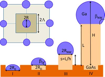
| The following image illustrates the parameters that the researchers used to describe the evolution of nanowire height and diameter. Initially, the gallium droplets exhibit a radius R0 at the base, which can be smaller than or equal to that of the hole. The contact angle of the droplets resting on the surface is denoted βD and should be close to 90°. During the incubation stage, most droplets just swell on the surface by increasing their base radius RD without changing much their contact angle, while almost no nanowires start. | |
 |
|
| Proposed scheme of Ga-catalyzed vapor-liquid-solid growth of GaAs nanowires in regular arrays: I, droplet predeposition (t = 0); II, formation of the initial nanowire monolayers after the incubation phase (t > 0); III, initial elongation of the nanowire and IV definition of the nanowire morphological parameters. (© ACS) | |
| "Interestingly" they write, "our statistical histograms do not show any pronounced asymmetry toward longer left tails. Instead, they are well-fitted by the double exponential shapes typical for macroscopic nucleation with a large critical length after which nanowires grow irreversibly." | |
| They also note that their model describes well the observed distribution shapes; however, unraveling the exact mechanisms of nanowires emerging from the substrate requires a separate study. | |
| Shortening the nucleation stage by increasing the As4 flux effectively narrows the size distribution. The results suggest that this parameter plays a key role for obtaining uniform arrays on silicon. | |
| "In addition, we believe that these results apply to other VLS growth using low surface energy metals such as Sn/Ga-catalyzed GaP nanowires or Sn/In-catalyzed InAs nanowires," the authors conclude their report. |
 By
Michael
Berger
– Michael is author of three books by the Royal Society of Chemistry:
Nano-Society: Pushing the Boundaries of Technology,
Nanotechnology: The Future is Tiny, and
Nanoengineering: The Skills and Tools Making Technology Invisible
Copyright ©
Nanowerk LLC
By
Michael
Berger
– Michael is author of three books by the Royal Society of Chemistry:
Nano-Society: Pushing the Boundaries of Technology,
Nanotechnology: The Future is Tiny, and
Nanoengineering: The Skills and Tools Making Technology Invisible
Copyright ©
Nanowerk LLC
|
|
|
Subscribe to a free copy of one of our daily Nanowerk Newsletter Email Digests with a compilation of all of the day's news. |