| Posted: Jul 27, 2017 | |
Observing electron beam etching atom by atom(Nanowerk News) Researchers have utilized electron beam irradiation to in situ etch CaO in a TEM, which permits simultaneous fabrication and imaging with atomic resolution. |
|
| This finding, reported in Nano Letters ("Electron Beam Etching of CaO Crystals Observed Atom by Atom"), gives insight into the etching mechanism; it is similar to a close-to-equilibrium process, as in chemical etching, leaving well-defined facets. | |
| Also, the etching preferentially takes place at {200} facets and leads to etch pits with favorable {111} facets. | |
| The morphology changes on the surfaces explain the origin of surface roughening, which is inevitable unless the diameter of the electron beam reaches the atomic level. | |
| Electron beam irradiation with high electron energies in the transmission electron microscope (TEM) has been applied to tailor materials with nanometric or even subnanometric precision. | |
| Unlike in electron beam induced etching (EBIE), atom displacements cause by knock-on collisions with the energetic electrons cannot be neglected so that the electron beam can also serve as an etching tool. This method does not lead to implantation or requires any gaseous precursors. | |
| Furthermore, in situ observation in the TEM can provide insight into the etching process, which allows researchers to investigate the roughening mechanism in detail. | |
 |
|
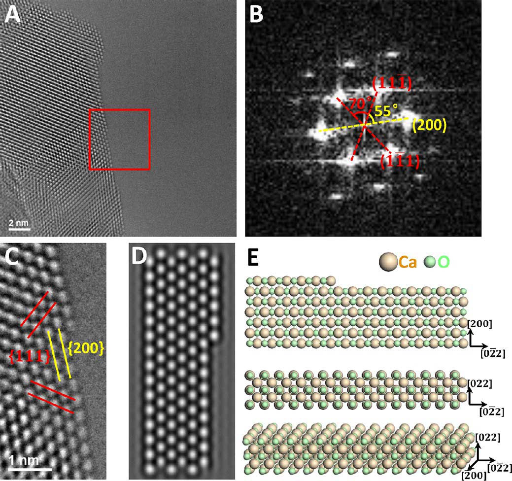
| Atomic structure of a CaO crystal: (A) HRTEM image of the CaO edge structure. (B) FFT of the image in the red square in (A). The red and yellow reflexes correspond to the {111} and {200} planes, respectively. (C) Magnified HRTEM image of the region labeled by red square in (A). (D) The corresponding TEM imaging simulation. (E) Stick-and-ball models of CaO, where the light yellow balls indicate the Ca atoms and the light green balls indicate the O atoms. (© ACS) (click on image to enlarge) | |
| Electron beam etching has already been used to sculpture nanostructures in different materials, including various metals (Au, Mg, Ni/Cr alloy), silica, graphene, molybdenum disulfide, and other transition-metal dichalcogenides. However, due to either the experimental limits or the material itself, it is difficult to record the specific etching processes at the atomic scale. | |
| The result of electron beam etching is similar to that of chemical etching although the atomic mechanisms are different. This present study on in situ electron beam etching has visualized the etching mechanism with atomic precision, which is of significant importance in the understanding of traditional etching and surface roughening. Because of the limits of CCD recording, the interval between the images is about 2-3 s, which limits the information about the temporal evolution. More insight could be gained by using high-speed direct electron recording. | |
| "In the future, higher control of the etching can be achieved by reducing the diameter of the electron beam down to the subnanometer scale, which could avoid the roughening of less favorable surfaces such as {001} by atomic-scale selectivity," the authors conclude their report. "Moreover, nanostructuring with single atom precision can be exploited through electron beam processing techniques." |
 By
Michael
Berger
– Michael is author of three books by the Royal Society of Chemistry:
Nano-Society: Pushing the Boundaries of Technology,
Nanotechnology: The Future is Tiny, and
Nanoengineering: The Skills and Tools Making Technology Invisible
Copyright ©
Nanowerk LLC
By
Michael
Berger
– Michael is author of three books by the Royal Society of Chemistry:
Nano-Society: Pushing the Boundaries of Technology,
Nanotechnology: The Future is Tiny, and
Nanoengineering: The Skills and Tools Making Technology Invisible
Copyright ©
Nanowerk LLC
|
|
|
Subscribe to a free copy of one of our daily Nanowerk Newsletter Email Digests with a compilation of all of the day's news. |