| Posted: Aug 09, 2017 | |
Scalable nanowire photonic crystals(Nanowerk News) Reporting their findings in Advanced Functional Materials ("Scalable Nanowire Photonic Crystals: Molding the Light Emission of InGaN"), researchers demonstrate the bottom-up synthesis of InGaN nanowire photonic crystals with precisely controlled size, spacing, and morphology, which can serve as the fundamental building blocks of a new generation of photonic crystal devices and systems. |
|
| Synthesizing InGaN nanowire photonic crystals via the bottom-up method, the formations of defects and dislocations are minimized due to the efficient surface strain relaxation. | |
 |
|
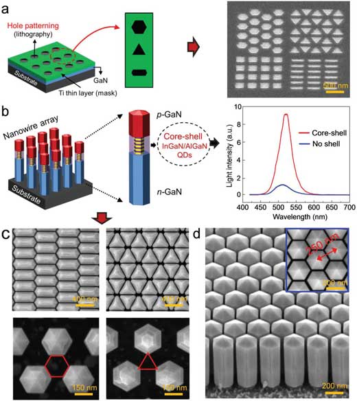
| a) Schematic illustration of hole-patterned Ti thin film mask for the selective-area epitaxy of InGaN photonic crystals. SEM image of various nanoscale patterns formed on the Ti mask is shown in the right panel. b) Illustration of bottom-up InGaN/AlGaN core–shell dot-in-nanowire array grown on pattered substrate. Photoluminescence spectrum of InGaN/AlGaN core–shell dot-in-nanowires measured at room-temperature (red curve) is shown in the right panel. Also shown for comparison is the photoluminescence emission of InGaN/GaN dot-in-nanowires without AlGaN shell (blue curve). c) Top-view SEM images of InGaN/AlGaN hexagonal dot-in-nanowire, nanotriangle, and nanorectangle arrays. d) 45°-tilted-view SEM image of the nanowire photonic crystals arranged in a triangular lattice with a lattice constant of 250 nm. The top-view SEM image is shown in the inset. (© Wiley-VCH Verlag) | |
| With the use of selective area epitaxy, the team demonstrates that the size, spacing, and morphology of InGaN photonic crystals, including dot-in-nanowires, nanotriangles, and nanorectangles, can be precisely controlled, and, as such, spatially extended band edge modes can develop over a large area of such defect-free photonic crystals. | |
| The researchers further observed that InGaN photonic crystals exhibit remarkably stable emission, compared to conventional InGaN light emitters. The luminescence emission, in terms of both the peak position (λ ∼ 505 nm) and spectral linewidths (full-width-half-maximum (FWHM) ∼ 12 nm), remained virtually invariant in the temperature range of 5–300 K and under excitation densities of 29 W cm-2 to 17.5 kW cm-2. | |
 |
|
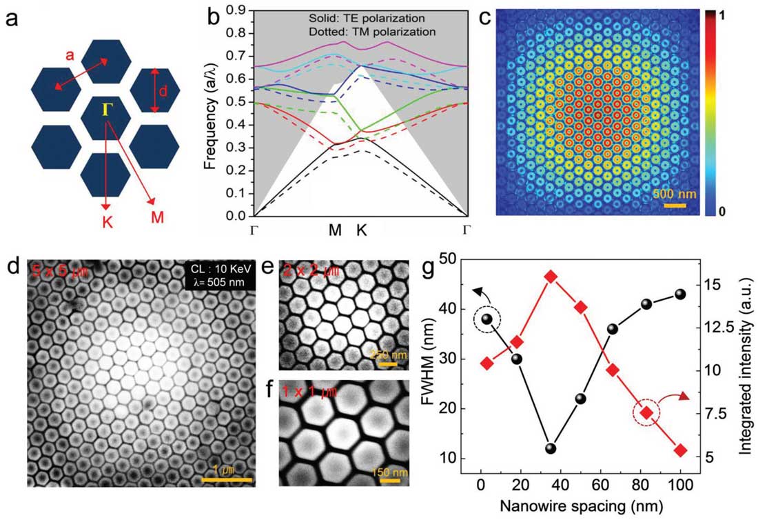
| a) Schematic diagram of the simulated photonic crystals, including the lattice constant a, nanowire lateral size d, and the reciprocal lattice vectors. b) Calculated photonic band structure of the 2D hexagonal array of nanowires (the corresponding SEM is shown in Figure 1d). c) The electric field profile of the band edge mode calculated by the 3D finite-difference time-domain method for a bands-edge mode (λ = 505 nm). d) Cathodoluminescence mapping image of an areal size of 5 × 5 µm2 measured at a wavelength of 505 nm. Cathodoluminescence mapping images over e) 2 × 2 µm and f) 1 × 1 µm regions, respectively. g) Variations of the integrated luminescence intensity and FWHM of InGaN photonic crystals versus nanowire spacing. (© Wiley-VCH Verlag) (click on image to enlarge) | |
| To appears to be the first demonstration of the absence of Varshni and quantum-confined Stark effects in wurtzite InGaN light emitters, factors that contribute significantly to the efficiency droop and device instability under high power operation. | |
| Such distinct emission properties of InGaN photonic crystals stem directly from the highly stable and scalable band edge modes, due to the precisely controlled size, position, and morphology of InGaN nanowire photonic crystals, and are ideally suited for uncooled, high-efficiency LED, and laser operation. | |
| "These unique characteristics, together with the scalable band edge optical mode, high light-extraction efficiency, on-demand beam characteristics, and full-color emission, render bottom-up GaN nanowire photonic crystals well suited for ultrahigh-efficiency, large-area LED and laser devices, as well as integrated nanophotonic circuits in the ultraviolet and visible spectral range," the authors conclude their report. |
 By
Michael
Berger
– Michael is author of three books by the Royal Society of Chemistry:
Nano-Society: Pushing the Boundaries of Technology,
Nanotechnology: The Future is Tiny, and
Nanoengineering: The Skills and Tools Making Technology Invisible
Copyright ©
Nanowerk LLC
By
Michael
Berger
– Michael is author of three books by the Royal Society of Chemistry:
Nano-Society: Pushing the Boundaries of Technology,
Nanotechnology: The Future is Tiny, and
Nanoengineering: The Skills and Tools Making Technology Invisible
Copyright ©
Nanowerk LLC
|
|
|
Subscribe to a free copy of one of our daily Nanowerk Newsletter Email Digests with a compilation of all of the day's news. |