| Posted: May 27, 2009 |
New gas sensor based on multiwalled carbon nanotubes |
|
(Nanowerk News) Argonne Center for Nanoscale Materials staff in the Nanofabrication & Devices Group together with collaborative users from the University of Wisconsin-Milwaukee have fabricated a miniaturized gas sensor using hybrid nanostructures consisting of SnO2 nanocrystals supported on multiwalled carbon nanotubes (MWCNTs) (Room-Temperature Gas Sensing Based on Electron Transfer between Discrete Tin Oxide Nanocrystals and Multiwalled Carbon Nanotubes).
|
|
In contrast to the high-temperature operation required for SnO2 nanocrystals alone, and to the insensitivity towards H2 and CO for CNTs alone, the hybrid sensor exhibits room-temperature sensing capability when exposed to low-concentration gases such as NO2, H2, and CO. The performance of the hybrid nanostructure sensor is attributed to the effective electron transfer between SnO2 nanocrystals and MWCNTs and to the increase in the specific surface area.
|
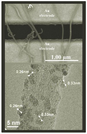 |
| Hybrid sensor fabrication process: (top) SEM image of a few MWCNTs spanning across two neighboring Au fingers of the interdigitated electrode; (bottom) HRTEM image of a MWCNT uniformly coated with SnO nanocrystals.
|
|
The hybrid platform as a sensing element provides an opportunity to engineer sensing devices with quantum-mechanical attributes due to the electron transfer. The nanomaterials employed are affordable, and the nanofabrication technique is simple and compatible with existing microfabrication capabilities; the latter, in turn, facilitates a scale-up process. This new sensing scheme will be instrumental for the development of new sensors based on hybrid nanostructures.
|