| Posted: June 18, 2009 |
The world's smallest trumpeter |
|
(Nanowerk News) Imagine how passionately this 0.00007 metre short musician blows the instrument toward the sky at dawn to make sound volume with his tiny breast. The height of his body is only about the diameter of a thick hair. The tube diameter of the trumpet looks about 0.0000001 metre (100 nanometres) and the length of it about 0.00001 metre (10 micrometres). This world smallest (maybe) standing statue of a musician has been fabricated as a part of a Nanotechnology MSc student project at the London Centre for Nanotechnology (LCN).
|
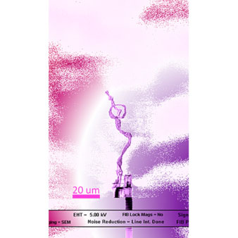 |
| Imagine how passionately he blows the instrument toward the sky to make sound with his tiny breast. This 0.00007 metre short sculpture happened to appear during advanced silicon etching with high-tech “plasma” process in a sealed vacuum chamber. His “chamber” music, therefore, unfortunately could not be transmitted physically outside his enclosed private room. Co-work with Mr Henry Crawford, a former Nanotechnology MSc, with co-supervisors Prof Ian Boyd and Dr Takashi Matsuura.
Scale bar shows 20 micrometres.
|
|
“This sculpture happened to appear during advanced silicon etching (ASE®) with high-tech “plasma” process in a vacuum chamber. Therefore, his “chamber” music could not be transmitted physically via vacuum outside his room, unfortunately,” says project supervisor, Dr Takashi Matsuura.
|
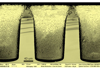 |
| Pints of beer. These are actually a little too small to quench your thirst. In order to make up a pint, you may need 200,000 fillings of these 0.24 mm-tall “glasses” made in silicon. This structure, actually a “via”, was formed in silicon by etching with an advanced “plasma” process in a vacuum chamber. Therefore, it is actually a “hot”, “dry” and “charged” process. This technology may be applied forwards micro-fluidic or micro-total-analysis-system (µTAS) applications, etc. Co-work with Mr Henry Crawford, a former Nanotechnology MSc, with co-supervisors Prof Ian Boyd and Dr Takashi Matsuura. Scale bar shows 40 micrometres.
|
|
This student project aimed at both nanofabrication of three dimensional artificial structures with plasma technologies and engineering application of them. Motivation of the project is: Demonstration of nanostructure fabrication capability over a few tens centimetre wide area is quite challenging as dimensional dynamic range spreads over millions. Adding the nanofabrication further with an artistic sense would draw wider public interests on nanotechnologies.
|
|
Not only this musician but also “icy glass for a pint of beer” and “Seabed creatures” have been created by a former MSc student Mr Henry Crawford during his experiments on plasma process optimisation. Although colorful and complex images are widely spread in the recent Nanoart world, this type of simple and monochromatic three dimensional (3D) sculptures may bring us nostalgia to classic and ease of mind.
|
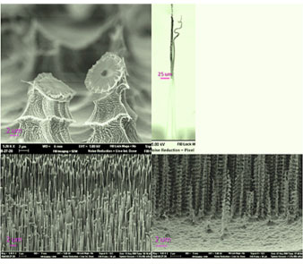 |
| Seabed Creature. These extremely tiny sculptures, resembling alien incubators (top left), a sea horse (top right), enoki-mushrooms (bottom left) and sea weed (bottom right), are all created by silicon etching with an advanced “plasma” process in a vacuum chamber, not in deep water. They are not living creatures “biologically”, but could perhaps work “electromechanically” in some future form. Co-work with Mr Henry Crawford, a former Nanotechnology MSc, with co-supervisors Prof Ian Boyd and Dr Takashi Matsuura.
|
|
“These kinds of novel 3D nanostructures are very interesting. The project also involves the study of the basic reaction mechanisms occurring at the atomic scale in the reaction schemes. It may also be possible to apply the fabricated structures to prototype test devices and to new device idea,” says co-supervisor Prof Ian Boyd.
|
|
Plasma is gas excited by radio frequency electric power into a complex mixture of ionized atoms and molecules as well as electrons and neutral radicals. A familiar example of plasma is one generated inside a fluorescent tube when it is turned on. More sophisticated plasma with particular reactive gases can realize this special fabrication in a carefully-designed vacuum chamber of the state-of-art instrument.
|
|
|
|
Plasma processing is currently the favoured tool for fabricating three dimensional nanostructures in planar technology, such as silicon integrate circuit technology, enabling the possibility of fabricating a wide variety of novel electronic, medical and MEMS devices. The plasma approach has the dual advantage of inducing directional chemical reactions due to linear acceleration of the ions produced by the bias voltage, and of lowering reaction temperatures due to the plasma-generated reactive species.
|
|
“Some may feel humor in this news as Blowing his own trumpet in English slang may mean exaggerating, but I hope this report is not and sounds smiling with receiving general acceptance,” adds Dr Takashi Matsuura.
|
|
About the London Centre for Nanotechnology
|
|
The London Centre for Nanotechnology, is a UK-based, multidisciplinary research centre forming the bridge between the physical and biomedical sciences. It was conceived from the outset with a management structure allowing for a clear focus on scientific excellence, exploitation and commercialisation. It brings together two world leaders in nanotechnology, namely University College London and Imperial College London, in a unique operating model that accesses the combined skills of multiple departments, including medicine, chemistry, physics, electrical and electronic engineering, biochemical engineering, materials and earth sciences, and two leading technology transfer offices.
|