| Posted: July 14, 2009 |
22nm interconnect technology takes a significant step forward |
|
(Nanowerk News) IMEC presents innovations in dielectrics and metallization technologies as well as in their integration approaches. Great progress has been obtained in the metallization of 22nm interconnects, in Cu/low-k reliability assessment and in the suppression of low-k integration damage. The results contribute to deliver the interconnect performance and reliability beyond the 32nm node.
|
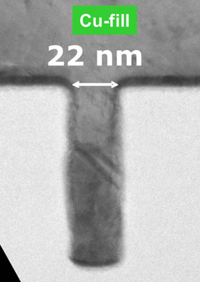 |
| Cross-section TEM inspection of a 22nm interconnect line.
|
|
Advanced metallization
|
|
IMEC researchers have investigated RuTa metallization as a promising scheme for achieving good metallization of 22nm features. It could likely replace the traditional Ta physical vapor deposition (PVD), which, for decreasing feature sizes, looses its ability to achieve uniform Cu seed. Four different metallization schemes (i.e., TaN/Ta, RuTa, TaN + Co and MnOx) were evaluated in terms of Cu fill, electrical performance and compatibility with chemical mechanical polishing (CMP) slurries. (Figure 1)
|
|
Barrier and dielectric reliability assessment
|
|
IMEC developed a model that for the first time describes the link between line edge roughness (LER) and time dependent dielectric breakdown (TDDB) lifetime. The model was validated on 50nm half pitch Cu damascene lines embedded into a k=2.5 low-k material, indicating that LER significantly contributes to the integrated dielectric reliability margin degradation. For older technology nodes, the reliability is mainly determined by dielectric deposition, patterning (lithography, etch/ash), barrier deposition, CMP and cap deposition, while for the 22nm and beyond the LER impact is expected to increase.
|
|
IMEC researchers also studied the stress of Cu interconnects inlayed into porous low-k and airgap structures. As a main trend, high porosity materials result in Cu with a lower stress, an effect which is less significant for narrow lines. Air gap structures show the lowest stress. This work is useful for interpreting reliability failure mechanisms and calibrating finite element models to predict stress in devices of future technology nodes.
|
|
IMEC demonstrated a unique test vehicle for assessing intrinsic reliability aspects of copper low-k interconnects and successfully used it for ranking different technology options. The test structure is also suited for studying the barrier/low-k interface, low-k plasma treatments, cleans, etc. It is expected that by using this test vehicle significant contribution will be made to the entire interconnect community by identifying and describing the fundamental reliability limits of copper/low-k metallization.
|
|
Plasma induced low-k damage reduction
|
|
IMEC proposes a non-contact dielectric constant metrology based on a near-field scanning probe microwave microscope to evaluate the dielectric properties after each processing step. The technique has been used to study the effect of plasma ash chemistry for removal of the photoresist mask and is shown to be a good method for non-invasive real-time in-line monitoring of patterned low-k structures at every step during interconnect integration. Plasma damage is the main cause of dielectric reliability loss in low-k materials during Cu/low-k integration. The introduction of porous low-k materials has increased the dielectrics sensitivity to plasma damage.
|
|
IMEC has also made good progress in developing alternative non-plasma routes for photo resist removal without attacking the low-k material. A particularly attractive approach is “all wet removal” since it mitigates the damage caused by dry ash. Among the methods, UV pretreatments followed by O3 and solvent treatments have resulted in full removal of post metal-hard-mask etch photoresist. Besides, radical anion based followed by O3 and gas expanded liquid processes show promising post-etch residue removal.
|
|
These results were obtained in cooperation with IMEC’s key parners in its core programs: Intel, Micron, Panasonic, Samsung, TSMC, Elpida, Hynix, Powerchip, Infineon, NXP, Qualcomm, Sony, ST Microelectronics.
|
|
|
|
About IMEC
|
|
IMEC is a world-leading independent research center in nanoelectronics and nanotechnology. IMEC vzw is headquartered in Leuven, Belgium, has a sister company in the Netherlands, IMEC-NL, offices in the US, China and Taiwan, and representatives in Japan. Its staff of more than 1650 people includes about 550 industrial residents and guest researchers. In 2008, its revenue (P&L) was EUR 270 million.
|
|
IMEC’s More Moore research aims at semiconductor scaling towards sub-32nm nodes. With its More than Moore research, IMEC looks into technologies for nomadic embedded systems, wireless autonomous transducer solutions, biomedical electronics, photovoltaics, organic electronics and GaN power electronics.
|
|
IMEC’s research bridges the gap between fundamental research at universities and technology development in industry. Its unique balance of processing and system know-how, intellectual property portfolio, state-of-the-art infrastructure and its strong network worldwide position IMEC as a key partner for shaping technologies for future systems.
|