| Posted: July 15, 2009 |
Development of thin-film electroluminescent device using inorganic oxides |
|
(Nanowerk News) Hiroshi Takashima and coworkers of the Superconducting Devices Group of the Nanoelectronics Research Institute, National Institute of Advanced Industrial Science and Technology (AIST) have developed red electroluminescent (EL) devices using thin-films of chemically stable perovskite oxides.
|
|
The thin-film EL devices use perovskite oxides, typified by barium titanate (BaTiO3), which has long been used as capacitor material for electronic circuits. With an emission starting voltage of ?10 V AC, the power source can be downsized due to low voltage operation of the device. A wide viewing angle is obtained by means of plane emission through the entire surface of the transparent electrode. There are no resource constraints due to the global abundance of required materials for the emitting and insulator layers. As all layers including the emitting layer are made of chemically stable inorganic materials, characteristic degradation due to oxidation or heat is unlikely to occur and thus a sealing process can be simplified. Hence, energy will be saved in a manufacturing process. Such applications as lighting, optical sources and displays will become feasible if higher brightness and polychromatic radiation are achieved in the years to come.
|
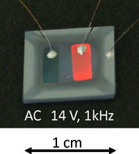 |
| Light emission from an inorganic EL device with perovskite oxides.
|
|
The results of this study will be published in the German scientific journal Advanced Materials.
|
|
Social Background for Research
|
|
Fluorescent lamps, today’s mainstream lighting equipment, pose an environmental load in that they use mercury. Alternative lighting that conserves energy is presently being developed, and the candidates are inorganic EL, organic EL and white LEDs. Organic EL devices entail several problems such as the tradeoff between brightness and life; degradation of characteristics by air exposure; cumbersome sealing process; and material cost. White LEDs are a promising candidate having achieved high brightness, but they present such problems as a limited viewing angle because they are a point light source, limitation of resources such as gallium, and high cost. On the other hand, inorganic EL devices using inorganic perovskite oxides have considerable merit because they have excellent chemical stability and heat resistance and are hardly degraded, and there is no limitation on resources, so there is strong demand for their development.
|
|
History of Research
|
|
The Nanoelectoronics Research Institute of AIST, has been studying new electronic phenomena and materials, and devices utilizing them, aiming the creation of innovative devices. Through these efforts, we discovered that many inorganic perovskite oxides efficiently emit fluorescence when excited with ultraviolet light. As we succeeded in fabricating a thin-film light emitting layer, we aimed at the development of a stable inorganic EL device having the emitting layer(s) stacked with insulator layers.
|
|
Details of Research
|
|
In the new inorganic EL device, as shown in Fig. 1, an insulator-/emitting-/insulator-layer stack was fabricated using the pulse laser deposition (PLD) method. For film deposition, an ArF excimer laser (wavelength 193 mm) was used at a substrate temperature of 700°C and in an atmosphere of 10 Pa oxygen. After annealing in the air, a transparent electrode was formed by PLD to perfect the EL device.
|
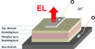 |
| Fig. 1 Schematic of the developed inorganic EL device. The emitting (phosphor) layer is sandwiched between insulator layers, and emission occurs when AC voltage is applied across the substrate and the transparent electrodes (top electrode). The emitted light passes through the transparent electrode.
|
|
Strontium titanate with 1% niobium added (1%Nb-SrTiO3) is used as the substrate electrode; calcium strontium titanate ((Ca0.6Sr0.4)TiO3), an inorganic perovskite oxide, is used as the light emitting layer containing a trace amount of praseodymium (Pr) added to the A sites as the emitting center; and strontium titanate (SrTiO3), another inorganic perovskite oxide, is used as the insulator layers. The thin films are deposited continuously to make a thin-film EL device with a double insulator layer structure. The top transparent electrode is made of ITO or SnO2 film. Oriented growth of all layers is confirmed by X-ray diffraction measurement.
|
|
Figure 2 (left) shows the emission spectrum of the inorganic EL device when AC voltage of 14 V, 1 kHz is applied. The emission is red, peaking at a wavelength of 612 nm. The photo shows that red light is uniformly emitted from the entire surface of the transparent electrode. This emission is very likely due to the energy transition from 1D2 to 3H4 of the Pr3+ ion. The emission starting voltage for this inorganic EL device is about 10 V, which is more than one order of magnitude smaller than those of existing inorganic EL devices. In addition, a thin-film EL device with double emitting layers is fabricated with a double insulator layer structure, and strong red emission is obtained with a voltage of 24 V (Fig. 2 (right)), which is approximately twice as large as that for the single-layer EL device, as discussed. A wide range of applications is expected for the newly developed low-voltage plane-emission EL devices.
|
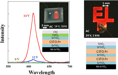 |
| Fig. 2 Emission spectra and photo of inorganic EL device emitting light. CSTO:Pr in the figure denotes perovskite oxide; ((Ca0.6Sr0.4)0.997Pr0.002)TiO3 for short. Left: Thin-film EL device with a single light emitting layer and double insulator layer structure. Emission is weak at 12 V near the wavelength 610 nm, with stronger emission at 14 V. Right: Thin-film EL device with double emitting layers and double insulator layer structure. Red-plane emission is observed at 24 V.
|
|
Future Schedule
|
|
To achieve practical use of the newly developed inorganic EL device with perovskite oxides, such as in the area of lighting, light sources and displays, we must improve the brightness, establish a technology for obtaining large-area devices at low cost, and realize multiple colors. We intend to pursue such technical targets as optimized emission characteristics and improved brightness, ways to obtain large-area devices at low cost and upgrade functionality, and the realization of RGB primary colors through the development of EL devices using other materials.
|