| Posted: July 20, 2009 |
Scientists directly observe formation of nanodot domain state |
|
(Nanowerk News) British and German scientists claim they have directly observed how domain states form in nanometre-scale ferroelectric crystals for the first time ("Domains in Ferroelectric Nanodots"). The team's work with barium titanate nanodots could now help ferroelectric random access memory (F-RAM) evolve to much higher data capacities.
|
|
F-RAM uses electric fields to physically move an atom within a crystal's unit cell. This atom remains in position when the field is removed, allowing it to store information. The strains that this process causes creates domain states, altered crystal orientations in the bulk structure. 'The operating voltage and speed of any ferroelectric memory depends on the number, shape and other characteristics of these domains,' explained Jim Scott of Cambridge University, who worked on the project.
|
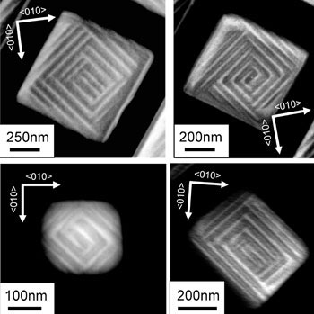 |
| Free-standing ferroelectric BaTiO3 nanodots form domain patterns shaped into quadrants of stripes. (Image: Nano Letters)
|
|
Fellow researchers at Queen's University, Belfast, cut nanodots from a BaTiO3 crystal using focused ion-beam milling. As free-standing crystals, these dots are free to move according to the forces they experience. The team saw that cooling through the Curie temperature - the point at which the material changes from being paraelectric to ferroelectric - arranged the dots into well-defined quadrants.
|
|
These observations have helped to test and refine simulations from Scott's Cambridge group and researchers at the University of Darmstadt, Germany. The team hopes that the improved understanding will now translate to other ferroelectric materials, like bismuth ferrite and lead zirconate titanate.
|
|
Information on nanometre scale behaviour of ferroelectric crystals is needed if companies like Panasonic, Fujitsu and Toshiba are to meet F-RAM's projected needs, Scott explains. Toshiba currently supplies the largest capacity F-RAM chips, at just 128 MB. The International Technology Roadmap for Semiconductors - drawn up by industry experts - states that this must increase to 1 GB by 2012, meaning that nanostructures must be used.
|
|
|
|
'This isn't curiosity-driven R&D - it is an industry ultimatum,' says Scott, who was a co-founder of pioneering F-RAM firm Symetrix. 'To make smaller ferroelectric memories, we need to know when these nanodomains will occur, how fast they move, and how much voltage is required to move them.'
|
|
Alexei Gruvermann, who studies ferroelectric materials at the University of Nebraska-Lincoln, US, agrees that these findings could help electronics manufacturers. 'Using single-crystalline free-standing nanoscale dots is a critical step forward in investigation of the scaling behaviour in ferroelectrics,' he said. However he points out that while free-standing dots are useful research tools, they are some way from the electronically-connected structures that would be used in memory chips.
|