| Posted: July 20, 2009 |
Berkeley Lab award winners promise cost-competitive solar cells and a 3-D look at nanoscale matter |
|
(Nanowerk News) Four of R&D Magazine’s prestigious R&D 100 Awards for 2009, which recognize the 100 most significant proven technological advances of the year, have gone to researchers at the U.S. Department of Energy’s Lawrence Berkeley National Laboratory and their colleagues.
|
|
“The Department of Energy’s national laboratories are incubators of innovation, and I’m proud they are being recognized once again for their remarkable work,” said Energy Secretary Steven Chu. ”The cutting-edge research and development being done in our national labs is vital to maintaining America’s competitive edge, increasing our nation’s energy security, and protecting our environment. I want to thank this year’s winners for their work and congratulate them on this award.”
|
|
The awards bring the total of Berkeley Lab’s R&D 100 wins to 52 plus two Editors Choice Awards over the years.
|
|
Cheryl Fragiadakis, who heads Berkeley Lab’s Technology Transfer and Intellectual Property Management Department, says, “To have all of these diverse technologies recognized is a reflection of the quality of scientific work we do at Berkeley Lab as well as the significance of its contribution to society. I am particularly pleased to note that three of this year’s winners are joint submissions with partners in the private sector, and all of the technologies are already being used or further developed by partners in the private sector.”
|
|
The 2009 award designees are:
|
|
EMGeo ElectroMagnetic Geological Mapper — the first commercially available technology for 3-D geophysical imaging of industrial-sized electromagnetic data. It will improve the hunt for energy sources.
Nanocrystal Solar Cells — the only solar cells that are long lasting and inexpensive enough to produce cost-competitive electricity.
NEXUS® DLC-X Coating System with Pulsed Filtered Cathodic Arc Technology — a system that promises more computer memory at less cost by depositing thin films of diamond-like carbon required by next-generation computer hard-disk heads.
TEAM Electron Microscope Stage — a device that enables atomic-scale imaging in 3-D. It holds and positions samples inside electron microscopes with unprecedented stability, position-control accuracy, and range of motion.
|
|
Mapping hydrocarbon reservoirs more cheaply and efficiently
|
|
Seismic imaging methods are used in hydrocarbon reservoir exploration, yet they have not proven effective in discriminating different types of reservoir fluids, such as brines, oil, and gas.
|
|
|
|
The EMGeo ElectroMagnetic Geological Mapper overcomes the technological problems involved in interpreting offshore hydrocarbon reservoirs by exploiting 21st century computing power —massively parallel computing resources — and combining it with advanced electromagnetic measurement techniques. The software was developed by Greg Newman and Michael Commer of Berkeley Lab’s Earth Sciences Division.
|
|
The technology offers oceanic subsurface mapping at a scale and resolution previously unavailable. It has proven useful in finding sources of alternative energy and in guiding environmental remediation. It will allow scientists to determine if an energy source exists before drilling for it, which could save millions of dollars in drilling costs, and help discover billions of dollars in oil and gas.
|
|
Cost competitive solar cells
|
|
The Nanocrystal Solar Cell is the first solar cell poised to be cost competitive with fossil fuels. It is also the first ultrathin solar cell based on dense nanocrystal films with no organic materials.
|
|
It was developed by Berkeley Lab Materials Sciences Division scientists Paul Alivisatos, Delia Milliron, Ilan Gur, Liberato Manna, Erik Scher, Haitao Liu, Steven Hughes, Neil Fromer, Richard Robinson, and Bryce Sadtler. Scientists from San Jose, CA-based Solexant also contributed.
|
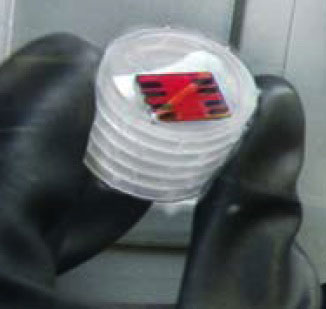 |
| Nanocrystal Solar Cells
|
|
The Berkeley Lab technology uses nanocrystals, which are essentially tiny semiconductor particles roughly 10 to 100 nanometers long. Like organic materials, nanocrystals can be synthesized in high volume and dispersed to allow for high-throughput solution-based processing. Nanocrystal Solar Cells perform the same function as conventional solar cells—turning sunlight into electricity—but at one-fifth the cost or less. Because of this dramatic cost savings, they have the potential to be the first photovoltaic cell to achieve widespread use in the energy market.
|
|
More computer memory at less cost
|
|
The total available storage in the world is projected to be roughly 600 exabytes by mid-2009. To cope with these demands, some 500 million hard disks were produced in 2007. The number is expected to pass the one billion mark in the ensuing five years.
|
|
The NEXUS DLC-X Coating System with Filtered Cathodic Arc Technology has the potential to make these products much better by increasing their capacity and decreasing their size, further reducing the cost per stored byte. It was developed by Andre Anders of Berkeley Lab’s Accelerator & Fusion Research Division and scientists from Veeco Instruments, Inc.
|
|
The technology applies dense, even, and unprecedentedly thin films of diamond-like carbon to the read/write head assemblies of computer hard disks. The pulsed, filtered cathodic arc delivers thinner coatings with the requisite evenness than chemical vapor deposition, ion beam, and sputtering techniques, or even previous cathodic arc techniques.
|
|
Atomic-scale imaging in 3-D
|
|
Three-dimensional atomic-resolution tomographic imaging requires analyzing a microscopic sample viewed from several directions, followed by a computerized reconstruction of the sample’s 3-D atomic structure. Such an exacting process has eluded researchers for decades, but is now possible with the Transmission Electron Aberration-corrected Microscope (TEAM) Stage. It holds and positions samples inside electron microscopes with unprecedented stability, position-control accuracy, and range of motion.
|
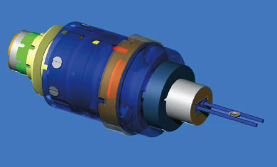 |
| TEAM Electron Microscope Stage
|
|
The technology was developed by Thomas Duden, Nord Andresen, Rich Weidenbach, and Andreas Schmid of Berkeley Lab’s Engineering and Materials Sciences Divisions. Scientists from Attocube Systems, FEI Company, and the University of Illinois at Urbana-Champaign also contributed.
|
|
The TEAM Stage will make one of the world’s most powerful electron microscopes even better, and enable previously impossible experiments. Trial-and-error detection of defects in a thin-film nanocrystal solar cell material may be minimized; and the fabrication of new biomaterials for longer-lasting artificial bone implants may be facilitated.
|
|
The R&D 100 Award-winning technologies were nominated by Berkeley Lab’s Technology Transfer and Intellectual Property Management Department. All winners of the 2009 award will receive a plaque at R&D Magazine’s formal awards banquet Nov. 12 in Orlando, FL.
|