| Posted: August 14, 2009 |
Nanowire and nanotube transistors for lab-on-a-chip applications |
|
(Nanowerk News) Nanostructures have the potential to transform the way we investigate life processes but only if we can find good ways to make them. Seunghun Hong, at Seoul National University, Korea, and colleagues discuss ways to integrate nanowires and nanotubes on chips (Nanowire and nanotube transistors for lab-on-a-chip applications – free access article).
|
|
Recent advances in nanotechnology have enabled high resolution chemical and biological detection - as sensors get smaller, their detection limit improves. So 1D nanostructures make ideal building blocks for sensors. These nanostructures, including nanowires (NWs) and single-walled carbon nanotubes (SWNTs), make it possible to detect individual molecules. For example, scientists have used SWNTs to measure the conductivity change caused by a single base pair mismatch in DNA. Combining these new components on lab-on-a-chip formats brightens the prospect for scientists developing advanced tools to investigate biochemical and life processes.
|
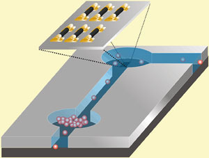 |
| Nanowire and nanotube-based transistors could be versatile components of lab-on-a-chip sensors
|
|
A major technological bottleneck holding back the practical applications of 1D nanostructure-based sensors has been the lack of ways to mass produce them. But in recent years, many researchers have demonstrated various promising mass fabrication methods. The selective growth strategy, where nanostructures are grown on patterns of catalysts, was one of the earliest growth concepts. While it enables scientists to position high purity structures at desired locations, it is more difficult on larger scales and does not work for some NWs. On the large scale, solution-phase synthesis is more promising as it requires cheaper equipment and lower temperatures. But the nanostructures must be directed to grow on specific locations and researchers have resorted to a variety of directed assembly strategies to achieve this. Electric fields, fluidic flows and magnetism have all been used as external guiding forces to align and position nanostructures.
|
|
Internal interactions can also be used. For example, scientists have functionalised solid substrates with self-assembled monolayers to create surface charge or polarisation that directs the absorption and alignment of NWs.
|
|
Although these methods have clearly shown the possibility for practical applications, assembling NWs and SWNTs on soft substrates, such as plastic, requires a different method. In this case, the assembly process must not involve high temperatures or reactive chemical treatments. And so printing technologies have emerged as a powerful tool. For example, by depositing NW solutions on a polymer stamp and blowing away the solvent, scientists made NW-inked stamps that could transfer the NWs on to the desired substrates.
|
|
Apart from practical applications, nanotechnology's largest contribution may be in opening up multidisciplinary science. Electronic devices previously unrelated to biotechnology are now being combined with biomolecules to make sensors capable of monitoring very low concentrations of disease-related molecules. It was only when the size of devices became comparable to that of biomolecules that the sensitivity really improved. Now scientists have made numerous biosensors using semiconductor NW or SWNT field effect transistors (FETs). Most NW FETs are made of silicon because its surface chemistry is well known and it is highly conductive, making it possible to create very sensitive sensors. But SWNTs are also attractive for sensors because they are even better at transporting electrons. The first generation of SWNT sensors is already on the market.
|
|
|
|
Reported nanotube sensors can be divided into two categories: those that contain a small number of semiconducting nanotubes and those that consist of SWNT networks. There is not yet a method to grow nanotubes with uniform chirality and so the yield of the devices in the first category is rather low - one needs chemical or electrical sorting to ensure single semiconducting behaviour. On the other hand, mass production of SWNT network devices is possible, but electrons move less easily through them.
|
|
In tandem with experiments, scientists are using modelling to try to understand the fundamental sensing mechanism of these FETs. They hope that by combining theoretical and experimental studies, they will be able to design NW and SWNT FETs that will be ideal candidates for future lab-on-a-chip components.
|