| Posted: January 8, 2007 |
EU funded project develops cost effective nanotechnology imprinting device |
|
(Nanowerk News) Finnish and French researchers working on an EU funded project have developed a nano-imprinting device for the mass production of solar cells and nano-scale bio-analysis platforms.
|
|
The nano-imprinting stepper uses a small patterned silicon chip as a stamp, the pattern of which is copied onto a polymer layer by imprinting. The polymer layer - made out of either thermoplastic or UV cured material - can then be used for replicating small sub-100 nm scale geometries onto larger areas.
|
|
Researchers say that the stepper may be suitable for nanopatterning optical and electronic materials and biomaterials, as well as three-dimensional replication.
|
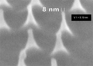 |
| Partial enlargement of a stamp. The projections shown in the image are less than 10 nanometer in size. Micronova's process equipment makes it possible to manufacture stamps even at this scale. (Image: VTT)
|
|
The new stepper uses Step and Stamp Imprint Lithography (SSIL), an ultra-miniaturised version of the decades-old embossing process in which a master tool - or a mould - is pressed into a soft material to create detailed patterns.
|
|
In the past, nano-scale geometries have been printed using e-beam lithography. Although effective for producing the tiniest stamp patterns, this technique is said to be much slower than the SSIL technique and unable to undertake large area processes.
|
|
The makers of the stepper also say that it is a much less expensive alternative to other microelectronics equipment that produce sub-100 nm line widths. Furthermore, traditional methods are not easily adaptable for printing on new functional materials or using 3D geometries.
|
|
The stepper was developed by researchers at Finland's VTT Technical Research Centre and France's SUS MicroTex S.A.S within the framework of the Emerging Nanopatterning Methods project. Funded under the Sixth Framework Programme (FP6), the project aims at standardising the nano-imprinting processes and establishing a process library.
|
|
The project has also been concerned with developing roll-to-roll methods for the production of nano-geometries. A printer designed by VTT combines the new nanopatterning method with gravure printing and flexo techniques in one process run. This printer is already used by VTT.
|