| Posted: November 9, 2009 |
Nanotechnology researchers find reliable, mess-free way to grow graphene |
|
(Nanowerk News) Single layers of carbon atoms, called graphene sheets, are lightweight, strong, electrically semi-conducting -- and notoriously difficult and expensive to make.
|
|
Now, a Cornell research team has invented a simple way to make graphene electrical devices by growing the graphene directly onto a silicon wafer. The work was published online Oct. 27 in the journal Nano Letters.
|
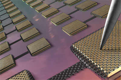 |
| A conceptual illustration of an array of single atom-thick graphene transistors.
|
|
Graphene is often hailed as potentially supplanting silicon in electronics, with its remarkable strength, despite its one atom-thick sheets, and its off-the-charts electrical properties. But making it in large quantities is a challenge, and scientists have turned to methods as crude as using scotch tape to pull off a layer of graphene from graphite, the material found in pencil lead. Such methods would never survive manufacturing, especially since it would produce graphene with varying numbers of layers at random positions.
|
|
"You can imagine trying to peel a piece of shrink wrap off a dish to put it on a new dish -- it's going to be messy," said lead researcher Jiwoong Park, Cornell assistant professor of chemistry and chemical biology.
|
|
Inspired by previous work in which scientists grew graphene on copper foil, the team grew the graphene directly onto silicon wafers coated with a special evaporated copper film. They then cut the graphene films into their desired shapes using such standard methods as photolithography, and removed the underlying copper with a chemical solution. What was left was a graphene film that draped down over the silicon wafer with little defect.
|
|
"Once the graphene is made on top of this wafer, you can apply any thin-film processing technique," Park said.
|
|
The team is now experimenting with growing full-scale, four-inch graphene wafers, which would further demonstrate the manufacturing potential of graphene-based electronics.
|
|
The paper's first author is Mark P. Levendorf, a graduate student in chemistry, and co-authors are Carlos S. Ruiz-Vargas, a graduate student in applied and engineering physics, and Shivank Garg '10, an undergraduate majoring in chemistry. The work was funded by the Defense Advance Research Projects Agency and the Cornell Center for Materials Research.
|