| Posted: January 20, 2010 |
Data storage: Memory boost on a wire |
|
(Nanowerk News) Demand for ultra-small, fast memories with high capacity is ever increasing but, because of architectural limitations, downscaling to dimensions smaller than 45 nm has become challenging. Now, Jia Fu, Navab Singh and co-workers at the A*STAR Institute of Microelectronics in Singapore have developed a new type of nanowire-based memory – dubbed TAHOS – which may circumvent this problem ("Integration of High-$kappa$ Dielectrics and Metal Gate on Gate-All-Around Si-Nanowire-Based Architecture for High-Speed Nonvolatile Charge-Trapping Memory").
|
|
Until now, one of the most successful types of non-volatile memories has been ‘flash’ memory. In this device, the information – in this case electrical charge – is stored in each memory cell on a floating gate that is programmed or erased by applying a voltage to a control gate. The information is then read by passing a current between the source and drain contacts through a channel situated under the floating gate, in a setup resembling a standard field-effect transistor.
|
|
Commenting on the challenges in downscaling conventional flash memories, Singh notes that: “The main issues with mainstream flash are the crosstalk between the cells due to inter-floating-gate coupling and leakage of stored charge on the floating gate.” One option is to replace the commonly used conducting silicon with non-conducting silicon nitride, as in silicon-oxide-nitride-oxide-silicon (SONOS) flash memories. Such devices, however, suffer from other scalability issues and low speeds.
|
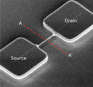 |
| Fig. 1: Scanning electron microscopy image of a wire-based TAHOS memory device connected to source and drain pads. (© IEEE)
|
|
The memory cell realized by Fu and his co-workers (Fig. 1) relies on an approach that employs a cylindrical, rather than planar, structure consisting of a silicon nanowire surrounded by various oxide layers and a wrap-around gate. This architecture is promising not only for scalability reasons, but also for improving device performance in terms of speed and power consumption. According to Singh, this is because of the hyperbolic-shaped electric field distribution in every insulating layer of the device, resulting from its cylindrical geometry.
|
|
A crucial aspect of the team’s memory cell is the choice of materials. The charge-trapping layer is made from hafnium dioxide, the blocking layer from aluminum oxide – both high-κ dielectrics – and the gate from tantalum nitride, giving the device its name, TAHOS. This combination of materials allows for higher speeds at lower voltages as a result of electric-field enhancement and its particular distribution across the device, in comparison with similar wire-based SONOS memory cells.
|
|
Singh notes, however, that: “The enhancement of the electric field in the tunnel oxide will have some impact on the retention properties and will have to be studied in more detail.” Thus, further work is required to pinpoint definitive applications for the TAHOS device as a next-generation memory.
|