| Posted: May 25, 2010 |
Researchers print field-effect transistors with carbon nanotube-infused ink |
|
(Nanowerk News) Rice University researchers have discovered thin films of nanotubes created with ink-jet printers offer a new way to make field-effect transistors (FET), the basic element in integrated circuits.
|
|
While the technique doesn't exactly scale down to the levels required for modern microprocessors, Rice's Robert Vajtai hopes it will be useful to inventors who wish to print transistors on materials of any kind, especially on flexible substrates.
|
|
In results reported last week in the online edition of ACS Nano ("Electrical Transport and Field-Effect Transistors Using Inkjet-Printed SWCNT Films Having Different Functional Side Groups"), Rice scientists working with researchers in Finland, Spain and Mexico have created nanotube-based circuitry using high-end ink-jet printers and custom inks.
|
 |
|
Vajtai, a faculty fellow in Rice's top-ranked Mechanical Engineering and Materials Science Department, led the study. Pulickel Ajayan, Rice's Benjamin M. and Mary Greenwood Anderson Professor in Mechanical Engineering and Materials Science and of chemistry, is a co-author.
|
|
The process involved the painstaking analysis of sample circuits printed with single-walled carbon nanotubes functionalized with four types of molecules. The researchers found that a single layer of nanotubes-infused ink printed onto a transparent foil didn't conduct electricity very well. But adding layers increased the connections between nanotubes, and so increased conductivity.
|
|
"The key is printing the appropriate number of layers to get the type of conduction you want, either metallic or semiconductive," Vajtai said, adding that researchers made no attempt to separate metallic from semiconducting nanotubes, which greatly simplified the process.
|
|
They found that at room temperature, electrical transport took place through the network of semiconducting and metallic nanotubes. At low temperatures, the semiconducting nanotubes became insulators, so electron tunneling between adjacent metallic nanotubes took over.
|
|
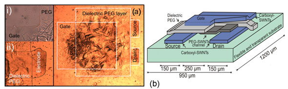
Ultimately, for building transistors, the team used two of the four studied mixtures of functionalized nanotubes as their building blocks. Nanotubes for conductive channels were treated with polyethylene glycol (PEG) while source, drain and gate electrodes were printed with carboxylated nanotubes. A layer of PEG was used as the gate dielectric.
|
|
"This is not a perfect transistor, but it is applicable in digital electronics," Vajtai said. "There are some limitations. I doubt anyone could take a $60 ink-jet printer and print predesigned electronic circuits. But with a high-end printer, it is a fairly straightforward process and allows you to put together whatever you want." He expects manufacturing nano-FETS in bulk would require a process more akin to silk-screening.
|
|
Though the researchers' test FETs were relatively large -- about a square millimeter -- they reported that circuits could scale down to about 100 microns, about the width of a human hair, with a channel length of about 35 microns – the size of the print head. Shrinking them further might be possible with smaller print heads or pretreated hydrophilic or hydrophobic surfaces.
|
|
Vajtai said nanotube-based FETs will be good for logic-based applications that can be printed on a flexible surface but don't need a large number of circuits. "Say you want to have a raincoat made with transistors – doing whatever a raincoat needs to do that requires electricity, such as controlling and analyzing signals from several sensors and light sources, for safety. It can be done.”
|
|
The paper's co-authors included primary author Eduardo Gracia-Espino of the Advanced Materials Department, Instituto Potosino de Investigacion Cientifica y Tecnologica, San Luis Potosi, Mexico; Giovanni Sala, Flavio Pino, Niina Halonen, Jani Mäklin, Géza Tóth, Krisztiçn Kordás and Heli Jantunen of the University of Oulu, Finland; Juho Luomahaara, Panu Helistö and Heikki Seppä of the VTT Technical Research Center of Finland; and Mauricio Terrones of the Universidad Carlos III of Madrid.
|