| Posted: May 26, 2010 |
Novel design promises a sensitive detector of hybrid particles that unite light and charge |
|
(Nanowerk News) Light can force the electrons at the surface of a metal to collectively oscillate. Coupling these oscillations with photons—creating 'surface plasmon polaritons' or SPPs—could lead to intriguing applications in communications, information processing and sensing since SPPs oscillate at very high frequencies that enable, potentially, the transfer of large volumes of data.
|
|
First, however, scientists need a way to efficiently capture SPPs. Now, Ping Bai and co-workers from the A*STAR Institute of High Performance Computing in Singapore have proposed and analyzed theoretically an electronic device that detects SPPs ("Electrical detection of plasmonic waves using an ultra-compact structure via a nanocavity").
|
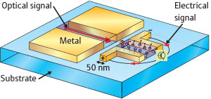 |
| Fig. 1: A schematic depiction of the proposed plasmonic detector that converts optical signals to electrical ones. Two L-shaped silver nanorods detect SPPs (red arrow) at the end of a waveguide and then enhance the electric-field intensity. A germanium active layer generates a photocurrent that is measured by an external circuit.
|
|
In the field of photonics, light is used to reproduce the functionality of electronics but at much higher speeds. However, while modern semiconductor processing can produce nanometer-size electronic devices, diffraction limits the size of optical components to approximately one micrometer. In plasmonics, the application of SPPs, the advantages of both are married. “Plasmonics allows light to propagate along sub-100 nanometer tracks and to be focused into a very small volume,” explains Bai. Plasmonics technology, however, is in its infancy, and researchers are still developing the basic components that engineers take for granted in electronics and photonics.
|
|
When SPPs come to the end of a metallic waveguide, for example, some of the energy is reflected backwards. The little energy that does escape decays very quickly in the gap between the guide and a detector. This makes SPPs difficult to measure.
|
|
The detector proposed by Bai and his co-workers consists of two L-shaped nanorods made of silver separated by a layer of germanium (Fig. 1). The parts of the L-shapes that run perpendicular to the propagating SPPs are closest to a waveguide, 50 nanometers away, and act like a nanoantenna. They focus the power of the plasmonic wave into the cavity formed by the other two arms of the Ls. This cavity amplifies the electric field. Finally, the enhanced electric field generates a photocurrent in the germanium that can be measured by an appropriate electrical circuit. “In this way, information can be transferred optically and then processed electrically, taking full advantage of both photonic and electronic technologies,” Bai notes.
|
|
The team’s simulations showed that the power absorbed from SPPs with a wavelength of 1.55 micrometers is at a maximum for an antenna length of 400 nanometers and a cavity gap of 75 nanometers. Bai says the next step is to fabricate an experimental prototype and to choose the proper materials and optimum structure for mass production.
|