| Posted: June 22, 2010 |
Imec demonstrates integrated electrical sources of surface plasmons |
|
(Nanowerk News) Metal-based nanophotonics (plasmonics) is a field concerned with manipulating and focusing light on nanoscale structures that are much smaller than conventional optic components. Plasmonic technology, today still in an experimental stage, has the potential to be used in future applications such as nanoscale optical interconnects for high performance computer chips, highly efficient thin-film solar cells, and extremely sensitive (bio)molecular sensors.
|
|
On the nanoscale, incoming light results in surface plasmon polaritons (SPPs), charge density oscillations at metal-dielectric interfaces. These have proven to be excellent markers for biochemical events, because they strongly enhance the local field near metal surfaces or nanostructures, and thus also the specific change induced by the presence of even ultrasmall quantities of biomolecules. Such a detection technique based on surface plasmon resonance (SPR) on thin gold films has already been successfully commercialized. But this technique still uses large external light sources and detectors.
|
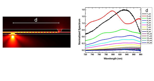 |
| Simulated (left) and experimental (right) coupling of the light emitted by a light-emitting diode (LED) into a MIM waveguide. The left figure shows the electric field profile that results of the coupling of a dipole emitter placed near a subwavelength slit in the bottom layer of the MIM waveguide. The emitted light couples efficiently to the plasmon waveguide mode and results in a standing wave pattern between two slits in the waveguide. This is also measured experimentally, as shown in the spectrally resolved output in the right figure for different lengths between the slits.
|
|
The state of the art in plasmonic waveguides has already been pushed forward substantially during the past years, demonstrating both plasmon propagation in low-loss long-range plasmon waveguides and highly confined plasmon propagation in e.g. metal-dielectric-metal waveguides. However, in order to incorporate such waveguides in realistic integrated circuits, they need to interface with fast and efficient electronics. But to do so, we'd need integrated electrical SPP sources and SPP detectors.
|
|
In recent publications in Nano Letters (De Vlaminck, Van Dorpe et al, 2007) and Nature Photonics (Neutens, Van Dorpe et al, 2009), imec has demonstrated the feasibility of efficient integrated detectors of surface plasmons. We have now extended this to integrated electrical sources of surface plasmons based on integrating light emitting diodes with metal-insulator-metal (MIM) waveguides. The strong measured polarization dependence, the experimentally obtained influence of the waveguide length, the measured spectral response are all in line with theoretical expectations.
|
|
Also surface plasmon polariton interference inside the waveguide is experimentally observed, which allowed us to reliably extract information about the wavelength and confinement of the propagating plasmons (illustrated in the figure). The realization of this building block completes the toolset that is needed to construct truly integrated electrically driven plasmonic circuits and hence paves the way for the integration of nanoscale plasmonic circuitry and integrated plasmonic biosensing.
|
|
This work has been published in the highly ranked journal Nano Letters: Neutens et al, Nano Lett. 2010, 10, 1429–1432.
|