| Posted: July 1, 2010 |
Transformation optics make a U-turn for the better |
|
(Nanowerk News) Powerful new microscopes able to resolve DNA molecules with visible light, superfast computers that use light rather than electronic signals to process information, and Harry Potteresque invisibility cloaks are just some of the many thrilling promises of transformation optics. In this burgeoning field of science, light waves can be controlled at all lengths of scale through the unique structuring of metamaterials, composites typically made from metals and dielectrics – insulators that become polarized in the presence of an electromagnetic field. The idea is to transform the physical space through which light travels, sometimes referred to as "optical space," in a manner similar to the way in which outer space is transformed by the presence of a massive object under Einstein's relativity theory.
|
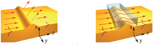 |
| Schematic on the left shows the scattering of surface plasmon polaritons (SPPs) on a metal-dielectric interface with a single protrusion. Schematic on right shows how SPP scattering is dramatically suppressed when the optical space around the protrusion is transformed. (Image courtesy of Zhang group)
|
|
So far transformation optics have delivered only hints as to what the future might hold, with a major roadblock being how difficult it is to modify the physical properties of metamaterials at the nano or subwavelength scale, mainly because of the metals. Now, a team of researchers with the U.S. Department of Energy (DOE)'s Lawrence Berkeley National Laboratory (Berkeley Lab) and the University of California (UC) Berkeley have shown it might be possible to go around that metal roadblock. Using sophisticated computer simulations, they have demonstrated that with only moderate modifications of the dielectric component of a metamaterial, it should be possible to achieve practical transformation optics results. The key to success is the combination of transformation optics with another promising new field of science known as plasmonics.
|
|
A plasmon is an electronic surface wave that rolls through the sea of conduction electrons on a metal. Just as the energy in waves of light is carried in quantized particle-like units called photons, so, too, is plasmonic energy carried in quasi-particles called plasmons. Plasmons will interact strongly with photons at the interface of a metamaterial's metal and dielectric to form yet another quasi-particle called a surface plasmon polariton(SPP). Manipulation of these SPPs is at the heart of the astonishing optical properties of metamaterials.
|
|
The Berkeley Lab-UC Berkeley team, led by Xiang Zhang, a principal investigator with Berkeley Lab's Materials Sciences Division and director of UC Berkeley's Nano-scale Science and Engineering Center (SINAM), modeled what they have dubbed a "transformational plasmon optics" approach that involved manipulation of the dielectric material adjacent to a metal but not the metal itself. This novel approach was shown to make it possible for SPPs to travel across uneven and curved surfaces over a broad range of wavelengths without suffering significant scattering losses. Using this model, Zhang and his team then designed a plasmonic waveguide with a 180 degree bend that won't alter the energy or properties of a light beam as it makes the U-turn. They also designed a plasmonic version of a Luneburg lens, the ball-shaped lenses that can receive and resolve optical waves from multiple directions at once.
|
|
"Since the metal properties in our metamaterials are completely unaltered, our transformational plasmon optics methodology provides a practical way for routing light at very small scales," Zhang says. "Our findings reveal the power of the transformation optics technique to manipulate near-field optical waves, and we expect that many other intriguing plasmonic devices will be realized based on the methodology we have introduced."
|
|
Zhang is the corresponding author of a paper describing this research that appeared in the journal Nano Letters, titled "Transformational Plasmon Optics." Co-authoring the paper with Zhang were Yongmin Liu, Thomas Zentgraf and Guy Bartal.
|
|
Says Liu, who was the lead author of the paper and is a post-doctoral researcher in Zhang's UC Berkeley group, "In addition to the 180 degree plasmonic bend and the plasmonic Luneburg lens, our approach should also enable the design and production of beam splitters and shifters, and directional light emitters. The technique should also be applicable to the construction of integrated, compact optical data-processing chips."
|
|
Zhang and his research group have been at the forefront of transformation optics research since 2008 when they became the first group to fashion metamaterials that were able to bend light backwards, a property known as "negative refraction," which is unprecedented in nature. In 2009, he and his group created a "carpet cloak" from nanostructured silicon that concealed the presence of objects placed under it from optical detection.
|
|
For this latest work, Zhang and Liu with Zentgraf and Bartal departed from the traditional transformation optics focus on propagation waves and instead focused on the SPPs carried in near-field (subwavelength) region.
|
|
"The intensity of SPPs is maximal at the interface between a metal and a dielectric medium and exponentially decays away from the interface," says Zhang. "Since a significant portion of SPP energy is carried in the evanescent field outside the metal, that is, in the adjacent dielectric medium, we proposed to control SPPs by keeping the metal property fixed and only modifying the dielectric material based on the transformation optics technique."
|
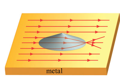 |
| In this schematic of a plasmonic Luneburg lens, a dielectric cone is placed on a metal to focus surface plasmon polaritons. (Image courtesy of Zhang group)
|
|
Full-wave simulations of different transformed designs proved the proposed methodology by Zhang and his colleagues correct. It was furthermore demonstrated that if a prudent transformational plasmon optics scheme is taken the transformed dielectric materials can be isotropic and nonmagnetic, which further boosts the practicality of this approach. The demonstration of a 180 degree bend plasmonic bend with almost perfect transmission was especially significant.
|
|
"Plasmonic waveguides are one of the most important components/elements in integrated plasmonic devices," says Liu. "However, curvatures often lead to strong radiation loss that reduces the length for transferring an optical signal. Our 180 degree bend plasmonic bend is definitely important and will be useful in the future design of integrated plasmonic devices."
|
|
Compared with silicon-based photonic devices the use of plasmonics could help to further scale- down the total size of photonic devices and increase the interaction of light with certain materials, which should improve performance.
|
|
"We envision that the unique design flexibility of the transformational plasmon optics approach may open a new door to nano optics and photonic circuit design," Zhang says.
|
|
This research was supported by the U.S. Army Research Office and the National Science Foundation's Nano-scale Science and Engineering Center.
|