| Posted: July 7, 2010 |
Nanomaterials: Making the right impression |
|
(Nanowerk News) Nanoporous anodic alumina films are versatile materials that can be used as templates in the fabrication of miniscule multifunctional objects for electronics and energy storage, such as nanotubes and nanowires. Unfortunately, the tedious small-scale techniques required to manufacture these films limits their implementation in industrial processes.
|
|
A team led by Tanu Kustandi from the A*STAR Institute of Materials Research and Engineering in Singapore has now developed a microfabrication procedure that is compatible with those used in the semiconductor industry to generate highly ordered nanoporous alumina films on large silicon wafers ("Wafer-Scale Near-Perfect Ordered Porous Alumina on Substrates by Step and Flash Imprint Lithography").
|
|
"Conventionally, films are prepared via a mechanical indentation approach, in which a master stamp is pressed onto an aluminum surface at very high pressure," explains Kustandi. However, this approach tends to break the underlying substrate that supports the aluminum films.
|
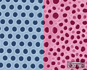 |
| Fig. 1: Scanning electron microscopy images of a highly ordered nanoporous alumina film obtained using the step-and-flash imprint process (left) and the amorphous film obtained without pre-patterning (right). (Image: T. Kustandi)
|
|
To avoid hard-stamping, Kustandi's team developed a 'soft' approach by combining a lithography process called step-and-flash imprint lithography (SFIL) with a wet-etching technique to pre-pattern the metal. First, they coated the silicon wafer with aluminum and an 'organic planarization layer' and sprayed the surface with an imprint resist—an etch-resistant low-viscosity material that polymerizes under ultraviolet light. Next, they positioned a quartz template patterned with nanometer-sized pillars on the surface, allowing the resist to contact and fill the template, then illuminated the assembly with ultraviolet light to create an inverse replica of the template. By moving the template toward an unpolymerized area and repeating the patterning process, the entire wafer was imprinted with nanometer-sized features.
|
|
After the researchers cleaned the patterned surface of residual and planarization layers, they transferred the pattern to the aluminum layer using an acid mixture as an etchant. Finally, they removed the polymer resist through ultraviolet–ozone treatment and oxidized the metal using an electrochemical process, known as anodization, to form the nanoporous alumina film.
|
|
Kustandi and his team generated a range of nanopore shapes, including squares and hexagons, by varying the structural configuration of the pillars. They discovered that SFIL patterning produced films with uniform pore sizes, shapes and arrangement, whereas non-patterned alumina appeared amorphous (Fig. 1). They also found that, unlike conventional techniques, the mild patterning conditions produced the nanometer-scale features with high repeatability and increased the longevity of the quartz template.
|
|
The researchers are currently investigating potential device applications for the nanoporous alumina films. "We are now utilizing the alumina template in the optoelectronics field to obtain high-efficiency gallium nitride-based light-emitting diodes," says Kustandi.
|