| Posted: July 10, 2010 |
Reducing lithography nanopatterns to 6 nanometers in size |
|
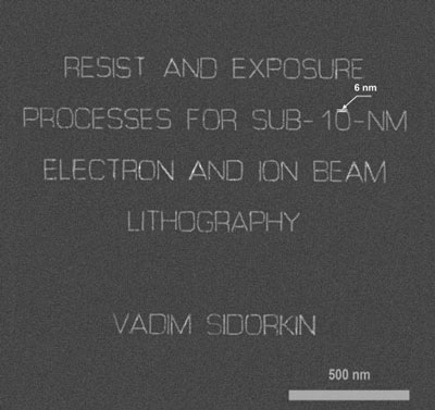
(Nanowerk News) NanoNed researcher Vadim Sidorkin is the first in the world to succeed in patterning a substrate with markings only 6 nanometres in size and only 14 nanometres apart. Vadim Sidorkin will gain his doctoral degree at TU Delft on 6 July. A spacing of 14 nanometres, would increase in the capacity of the memory chips of, for example, new generation mobile phones tenfold.
|
|
Sidorkin researched into creating the smallest possible structures using electron beams and ion beams. At the present time the industry generally uses light beams to etch extremely small structures onto semiconductor material, for instance in the manufacture of computer chips. Sidorkin used a Helium Ion Microscope (HIM), purchased by TNO with NanoNed funds, to create helium beams, and using this technique he was able to draw dots having a diameter of only six nanometres.
|
 |
|
Mobile phones
|
|
In building nanostructures it is not only important how small you can make individual lines and dots, but also how close together you can make them, because of the demand for ever-higher data storage densities within, for instance, the newest generations of mobile phones. The spacing of 14 nanometres that Sidorkin achieved could increase their data storage capacity by a factor ten. To allow the distance between separate patterns to be reduced to a minimum, the Russian researcher used an ultra-thin hydrogen silsequioxane (HSQ) lacquer that was developed specially for this purpose by TU Delft.
|
|
Helium ion beam
|
|
Sidorkin compared the performance of the helium ion beam with an electron beam, and found that using helium ions made it possible to etch structures much closer together. Since helium ions are larger and heavier than electrons, they can be fired at the substrate surface with less speed and still deliver the same collision energy. As the result helium ions also do much less damage to the surrounding material, because they rebound less far off the surface and penetrate sideways less far into the structure itself.
|
|
Lithography
|
|
To make a computer chip, silicon wafers are first coated with a thin layer of lacquer called photoresist. This layer is then exposed to light in the pattern desired, using a laser, an electron beam or an ion beam. Electron beams and ion beams are much slower in operation than are laser beams, but they can 'write' much smaller patterns onto the lacquer layer. The wafer is then treated so that only the lacquer that was exposed to the ion beam remains.
|
|
NanoNed
|
|
NanoNed is a national nanotechnology initiative that brings together Dutch strengths in nanoscience and nanotechnology, in a national network of scientific, economic and socially relevant research and infrastructure projects. The NanoNed secretariat is housed by the Technology Foundation (STW).
|