| Posted: July 13, 2010 |
Observation of atomic processes identifies how fullerenes push their way under graphene surfaces |
|
(Nanowerk News) Fullerene and graphene, two forms of carbon only recently discovered, have been stimulating the imaginations of researchers ever since their discovery (fullerene in 1970, graphene in 2004). With graphene especially, researchers see a chance for a new chapter in electronics, since this semiconductor material could one day replace the long-standing key element silicon. For this to happen, it would have to be possible to dope graphene – which is a single-atom layer of graphite – with foreign atoms. And in such a way that the important structural properties of graphene remain intact.
|
|
In the online preprint of August issue of the journal Advanced Materials ("Imaging Buried Molecules: Fullerenes Under Graphene") researchers from Helmholtz-Zentrum Berlin für Materialien und Energie (HZB) report on a new technique of microscopy. With it, they can show how individual fullerene molecules used for doping push their way under a graphene layer that has been previously deposited onto a nickel substrate.
|
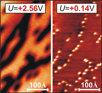 |
| Microscopical image of a graphene layer on a nickel substrate. The image to the left, which was measured at an arbitrary bias voltage of the microscope tip, shows just dark stripes. Only after the bias voltage has spectroscopically been tuned to the very C60 molecules (right), they become visible beneath the graphene layer as the cause of the stripe pattern.
|
|
Graphene is the first crystal known to be stable in two dimensions, because its carbon atoms arrange themselves into a honeycomb structure of hexagons. Fullerene has the addition of pentagons, allowing a spherical structure for which the 60-carbon-atom molecule has made its name as the soccer ball molecule.
|
|
Andrei Varykhalov and colleagues deposited a thin layer of graphene onto a nickel substrate using chemical vapour deposition starting with propylene. Next, they inserted individual fullerene molecules between the nickel surface and the graphene layer. They achieved this by rapidly heating the sample to 400 degrees Celsius, followed by brief annealing. The crucial technique that allowed them to observe the fullerene molecules as they squeezed their way in – a process called intercalation – was scanning tunnelling microscopy.
|
|
An electrically conductive stylus tip is systematically scanned over the sample surface, which is also conductive. Yet, the tip and object surface never come into contact, so no current flows at first. When the microscope tip comes to within a few tenths of a nanometre of the sample surface, however, the tunnel-ling effect kicks in. That means an exchange of electrons from the sample sur-face and tip starts to take place. If a voltage is then applied, a tunnel current flows, which responds with utmost sensitivity to the tiniest changes in distance.
|
|
The HZB researchers set up their scanning tunnelling microscopy experiment such that a clear contrast shows up as soon as the tip of the microscope per-ceives the fullerene molecules beneath the graphene surface. To obtain crucial parameters for this, they first studied the sample using synchrotron radiation at the storage ring BESSY II.
|
|
"Using our imaging technique, we can visualize intercalation compounds quite universally," Andrei Varykhalov emphasizes the importance of the experiments. In the development of new semiconductor technology, such an imaging tech-nique is indispensable for developing new components.
|
|
The Helmholtz-Zentrum Berlin für Materialien und Energie (HZB) operates and develops large scale facilities for research with photons (synchrotron beams) and neutrons. The experimental facilities, some of which are unique, are used annually by more than 2,500 guest researchers from universities and other research organisations worldwide. Above all, HZB is known for the unique sam-ple environments that can be created (high magnetic fields, low temperatures). HZB conducts materials research on themes that espe-cially benefit from and are suited to large scale facilities. Research topics include magnetic materials and functional materials.
|
|
In the research focus area of solar energy, the development of thin film solar cells is a priority, whilst chemical fuels from sunlight are also a vital research theme. HZB has approx.1,100 employees of whom some 800 work on the Lise-Meitner Campus in Wannsee and 300 on the Wilhelm-Conrad-Röntgen Campus in Adlershof.
|