| Posted: July 13, 2010 |
Record efficiencies for large-area epitaxial thin-film silicon solar cells |
|
(Nanowerk News) IMEC realized large-area (70cm2) epitaxial solar cells with efficiencies of up to 16.3% on high-quality substrates. And efficiencies of up to 14.7% were achieved on large-area low-quality substrates, showing the potential of thin-film epitaxial solar cells for industrial manufacturing. The results were achieved within imec's silicon solar cell industrial affiliation program (IIAP) that explores and develops advanced process technologies aiming a sharp reduction in silicon use, whilst increasing cell efficiency and hence further lowering substantially the cost per Watt peak.
|
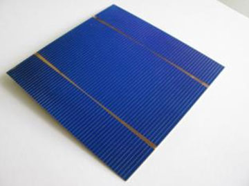 |
| Imec large-area (70cm2) epitaxial solar cell with an efficiency of up to 16.3% on high-quality substrate.
|
|
Besides wafer-based bulk silicon solar cells imec aims at developing epitaxial thin-film (<20µm) silicon solar cells grown on low-cost silicon carriers within its silicon solar cell IIAP.. The epitaxial thin-film process on low-cost silicon carriers is generically similar to the bulk process and the epi-process can be implemented with limited equipment investment in an existing crystalline silicon solar cell manufacturing line. To improve the optical confinement of light in the active part of the cell, a buried porous Si reflector is developed.
|
|
Imec realized 20µm thick high-quality epitaxial silicon stacks both on top of a highly-doped high-quality substrate and on a low-cost, UMG (upgraded metallurgic grade)-type, multi-crystalline Si substrate. The p+-type back surface field (BSF), the p-type base and the n-type front-side emitter were grown by chemical vapor deposition. The light-trapping scheme consists of plasma texturing of the front surface in combination with an internal porous silicon Bragg reflector positioned at the epitaxial/substrate interface. The cells on the high-quality substrate are contacted with copper plating. For the cells made on the low-quality substrates, the metallization is realized with screenprinting, which is the final step after the formation of the diffused front surface field (FSF) and the silicon nitride antireflection coating. In this way, the epitaxially grown 'wafer equivalent' substrates are fully compatible with standard industrial (bulk) solar cell processing.
|
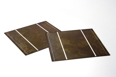 |
| Imec epitaxial thin-film silicon solar cell on low-quality substrate with screen printed metal lines achieving efficiencies of up to 14.7%.
|
|
"These efficiencies of up to 16.3% on high-quality substrates and of up to14.7 % on low-cost substrates show that industrial-level efficiencies are within reach for this technology;" said Jef Poortmans, director imec energy/solar program. "By implementing copper-based contact schemes, we can further increase the efficiency making epitaxial thin-film silicon solar cells on low-cost wafers an interesting industrial technology."
|
|
About imec
|
|
Imec performs world-leading research in nanoelectronics. Imec leverages its scientific knowledge with the innovative power of its global partnerships in ICT, healthcare and energy. Imec delivers industry-relevant technology solutions. In a unique high-tech environment, its international top talent is committed to providing the building blocks for a better life in a sustainable society. Imec is headquartered in Leuven, Belgium, and has offices in Belgium, the Netherlands, Taiwan, US, China and Japan. Its staff of more than 1,750 people includes over 550 industrial residents and guest researchers.
|