| Posted: September 1, 2010 |
Nanolithography: One-shot spots |
|
(Nanowerk News) Demand for ever-smaller electronic devices, whether are for information storage, high-definition displays or sensor arrays, is driving demand for nanofabrication techniques that can define ever-smaller features on circuit boards — on scales smaller than micrometers, or even nanometers, in diameter.
|
|
Electron beam and X-ray lithography are well-established techniques for nanofabrication, but both have disadvantages, especially in terms of cost and flexibility. On the contrary, optical lithography is generally cheap and adaptable, but it does not allow the fabrication of features smaller than a few hundred nanometers. This limitation can be overcome by applying a technique known as near-field enhanced laser irradiation, whereby the light of optical beams is concentrated in a spatial region much smaller than the wavelength when it scatters on a nanostructure. The degree of improvement is determined by the dimensions of the nanostructures and the distance from its surface.
|
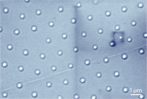 |
| Fig. 1: Scanning electron microscope image of the fabricated silicon nanobump arrays.
|
|
Using optical lithography, Xincai Wang from A*STAR's Singapore Institute of Manufacturing Technology and co-workers have now fabricated arrays of 'nanobumps' surrounded by ring-shaped trenches on a silicon substrate ("Fabrication of silicon nanobump arrays by near-field enhanced laser irradiation").
|
|
Wang and his co-workers deposited a hexagonal array of silica microspheres on a silicon substrate and irradiated it with single shot from an ultravioilet laser. The resultant trenched nanobumps — obtained under specific laser power conditions — were about 160 nanometers wide and 40 nanometers tall (Fig. 1). Their formation was linked to near-field laser scattering on the silica microspheres, given that they are arranged in the same exact way. The capabilities of near-field enhanced laser irradiation had been explored before, but most of the previous work has been on the fabrication of nanoscale pits or dents.
|
|
According to the team, the formation of such bumps and trenches stems from the way in which silicon resolidifies after being melted in the focal area generated by the microspheres. Silicon has a lower density in the solid phase, so when resolidification starts from the edges of the molten area, the remaining liquid is pushed towards the center, eventually creating the bump. This explanation is supported by the observation that the volume of the trench is very similar to that of the bumps, the team notes.
|
|
"Compared with other nanofabrication techniques, the developed process is simple and straightforward," says Wang. He believes that the silicon nanobumps could find application in sensitive detectors, efficient photovoltaic cells, field-emitter arrays and displays.
|