| Posted: Oct 08, 2010 |
|
Single-crystal films could advance solar cells
|
|
(Nanowerk News) Cornell researchers have developed a new method to create a patterned single-crystal thin film of semiconductor material that could lead to more efficient photovoltaic cells and batteries.
|
|
The "holy grail" for such applications has been to create on a silicon base, or substrate, a film with a 3-D structure at the nanoscale, with the crystal lattice of the film aligned in the same direction (epitaxially) as in the substrate. Doing so is the culmination of years of research by Uli Wiesner, professor of materials science and engineering, into using polymer chemistry to create nanoscale self-assembling structures.
|
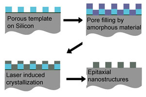 |
| Amorphous silicon, deposited on a porous template fills the empty spaces. Laser heating melts the deposit and the top few microns of the silicon substrate. In a few nanoseconds the melted silicon recrystallizes. The substrate acts as a seed crystal for the material above, causing it to crystallize with the same alignment. This makes it easier for electric charges to flow, making possible more efficient solar cells and batteries.
|
|
He and his colleagues report the breakthrough in the Oct. 8 issue of the journal Science. They used the new method to create a film with a raised texture, made up of tiny pillars just a few nanometers across. "Just the ability to make a single-crystal nanostructure has a lot of promise," Wiesner said. "We combine that with the ability of organic polymer materials to self-assemble at the nanoscale into various structures that can be templated into the crystalline material." (A nanometer -- nm -- is a billionth of a meter, about three atoms wide.)
|
|
Wiesner's research group previously used self-assembly techniques to create Gräetzel solar cells, which use an organic dye sandwiched between two conductors. Arranging the conductors in a complex 3-D pattern creates more surface area to collect light and allows more efficient charge transport, Wiesner said.
|
|
Performance improves the most when the conducting materials are single crystals, Wiesner said. Most techniques for creating such films produce polycrystalline material -- a collection of "grains" or small crystals bunched together at random -- and grain boundaries retard the movement of electric charges, he explained.
|
|
Wiesner's method uses block co-polymers to create porous templates into which a new material can flow and crystallize. A polymer consists of organic molecules that link into long chains to form a solid. A block co-polymer is made by joining two different molecules at their ends. When they chain together and are mixed with metal oxides, one forms a nanoscale pattern of repeating geometric shapes, while the other fills the space in between. Burning the polymer away leaves a porous metal oxide nanostructure that can act as a template.
|
|
Wiesner's team created a template with hexagonal pores on a silicon single-crystal substrate and deposited films of amorphous silicon or nickel silicide over it. In collaboration with Mike Thompson, associate professor of materials science and engineering, they then heated the silicon surface with very short (nanosecond) laser pulses. This melts the newly deposited layer and the top few microns (millionths of a meter) of the silicon substrate. After only a few tens of nanoseconds the molten silicon recrystallizes with the single crystal silicon substrate acting as a seed crystal to trigger crystallization in the deposited material above it, causing that crystal to line up epitaxially with the seed.
|
|
The template is dissolved away, leaving an array of hexagonal pillars about 30 nm across. The team has made porous nanostructured films up to 100 nm thick with other complex shapes. In previous work Wiesner created lattices of cylinders, planes, spheres and complex "gyroids" by varying the composition of co-polymers.
|
|
Other materials could be deposited, the researchers said. The goal here, they said, was to demonstrate the formation of film with the same material as the substrate (officially known as homoepitaxy) and with a different material (heteroepitaxy).
|
|
In a further proof-of-concept experiment, the researchers showed that the structured thin film could be arranged in micron-scale patterns, as might be necessary in designing an electronic circuit, by laying a mask over the surface before applying laser heating.
|
|
"We have essentially gotten to the holy grail," Wiesner said. "It is not only a nanostructured single crystal, but it has an epitaxial relation to the substrate. There is no better control."
|
|
The research was supported by the National Science Foundation, Department of Homeland Security and Cornell's Energy Materials Center, funded by the U.S. Department of Energy.
|