| Posted: Oct 21, 2010 |
|
Imec coordinates R+D for the integrated production of photovoltaic modules based on ultra-thin crystalline Si
|
|
(Nanowerk News) Imec has started work, together with its project partners, on SUGAR, a project under the EU's 7th framework program for ICT. The project's goal is to develop a process for the integrated production of photovoltaic modules based on ultra-thin crystalline Si. This includes finding a way to produce 50µm thin crystalline Si, and a process to fabricate modules from this ultra-thin Si with state-of-the-art conversion efficiency. Imec is SUGAR's project coordinator; the other partners are 4PICO (Netherlands), Applied Materials Baccini (Italia), Ferro (Netherlands), Bosch Rexroth (Netherlands), Dow Corning Europe (Belgium), Universidade De Lisboa (Portugal), Semilab (Hungary), Cemef-Mines (France), and Fraunhofer (Germany).
|
|
The optimal thickness of solar cells made from mono-crystalline Si is around 50µm. Reducing the thickness of solar cells from the current de-facto standard of 180µm to 50µm would result in modules that are approximately 10% cheaper. The SUGAR project aims to solve the two main technological challenges that stand in the way of reaching that cost reduction. One is to produce solar wafers of 50 microns, and the second one is to process them into solar cells.
|
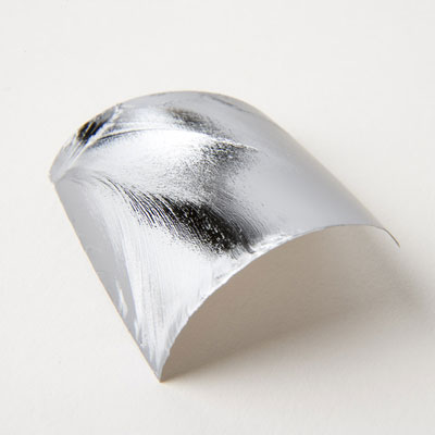 |
| Ultra-thin Si foil, detached from Si tile with SLiM-cut.
|
|
Fabricating 50µm thick wafers
|
|
The first goal of SUGAR is to develop a prototype line that takes Si tiles (wafers with a thickness above 1cm) as input, and that outputs large-area (50cm²) ultra-thin wafers (~50µm). The line would have a target throughput of 100 wafers per hour, and the wafering process should be with minimal kerf loss.
|
|
The basis of that line will be an innovative and proven method, nicknamed SLiM-cut. With SLiM-cut, a high-stress field is applied to a Si wafer so that a crack propagates in the Si substrate parallel to the surface at a given depth. The top Si layer is separated from the parent substrate and processed into a solar cell. The parent substrate can be re-used for further wafering.
|
|
To apply the stress, a material (e.g. a metal) with a thermal expansion coefficient different from Si is deposited and bonded at a high temperature on top of the thick crystalline Si wafer. When the wafer cools down, the mismatch of the thermal expansion coefficient between the top material and the Si induces the stress field. This field initiates and propagates a crack in the Si, close to and parallel with the surface. Next, the top layer of the Si and the attached metal layer snap off from the parent substrate. The metal layer is removed from the Si foil in a metal-etching solution, resulting in a clean and stress-free ultra-thin Si foil. The substrate can be re-used to peel off further layers.
|