| Nov 23, 2010 |
Scientists crack materials mystery in vanadium dioxide
|
|
(Nanowerk News) A systematic study of phase changes in vanadium dioxide has solved a mystery that has puzzled scientists for decades, according to researchers at the Department of Energy's Oak Ridge National Laboratory (ORNL).
|
|
Scientists have known that vanadium dioxide exhibits several competing phases when it acts as an insulator at lower temperatures. However, the exact nature of the phase behavior has not been understood since research began on vanadium dioxide in the early 1960s.
|
|
Alexander Tselev, a research associate from the University of Tennessee-Knoxville working with ORNL's Center for Nanophase Materials Sciences, in collaboration with Igor Luk'yanchuk from the University of Picardy in France used a condensed matter physics theory to explain the observed phase behaviors of vanadium dioxide, a material of significant technological interest for optics and electronics.
|
|
"We discovered that the competition between several phases is purely driven by the lattice symmetry," Tselev said. "We figured out that the metallic phase lattice of vanadium oxide can 'fold' in different ways while cooling, so what people observed was different types of its folding."
|
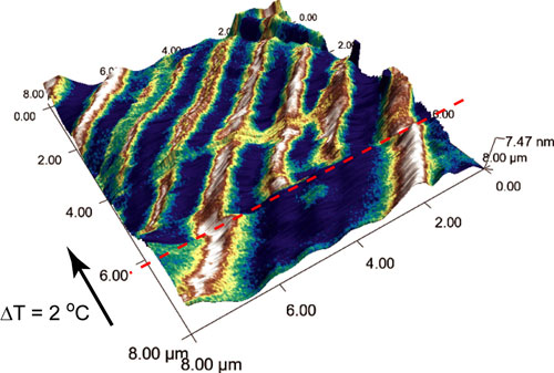 |
| Theoretical research at Oak Ridge National Laboratory can help explain experimental results in vanadium dioxide, such as the formation of thin conductive channels (seen in white) that can appear under strain in a nanoscale vanadium dioxide sample.
|
|
Vanadium dioxide is best known in the materials world for its speedy and abrupt phase transition that essentially transforms the material from a metal to an insulator. The phase change takes place at about 68 degrees Celsius.
|
|
"These features of electrical conductivity make vanadium dioxide an excellent candidate for numerous applications in optical, electronic and optoelectronic devices," Tselev said.
|
|
Devices that might take advantage of the unusual properties of VO2 include lasers, motion detectors and pressure detectors, which could benefit from the increased sensitivity provided by the property changes of vanadium dioxide. The material is already used in technologies such as infrared sensors.
|
|
Researchers said their theoretical work could help guide future experimental research in vanadium dioxide and ultimately aid the development of new technologies based on VO2.
|
|
"In physics, you always want to understand how the material ticks," said Sergei Kalinin, a senior scientist at the CNMS. "The thermodynamic theory will allow you to predict how the material will behave in different external conditions."
|
|
The results were published in the American Chemical Society's Nano Letters. The research team also included Ilia Ivanov, John Budai and Jonathan Tischler at ORNL and Evgheni Strelcov and Andrei Kolmakov at Southern Illinois University.
|
|
The team's theoretical research expands upon previous experimental ORNL studies with microwave imaging that demonstrated how strain and changes of crystal lattice symmetry can produce thin conductive wires in nanoscale vanadium dioxide samples.
|
|
This research was supported in part by the Department of Energy's Office of Science and by the National Science Foundation. Researchers also used instrumentation at the Office of Science-supported Center for Nanophase Materials Sciences and Advanced Photon Source User Facilities at Oak Ridge and Argonne national laboratories, respectively.
|
|
CNMS is one of the five DOE Nanoscale Science Research Centers, premier national user facilities for interdisciplinary research at the nanoscale supported by the DOE Office of Science. Together the NSRCs comprise a suite of complementary facilities that provide researchers with state-of-the-art capabilities to fabricate, process, characterize and model nanoscale materials, and constitute the largest infrastructure investment of the National Nanotechnology Initiative. The NSRCs are located at DOE's Argonne, Brookhaven, Lawrence Berkeley, Oak Ridge and Sandia and Los Alamos National Laboratories. For more information about the DOE NSRCs, please visit http://nano.energy.gov. ORNL is managed by UT-Battelle for the Department of Energy's Office of Science.
|