| Dec 18, 2010 |
High-quality III-V layers on Si(001) pave the way to high-performance Ge/III-V CMOS
|
|
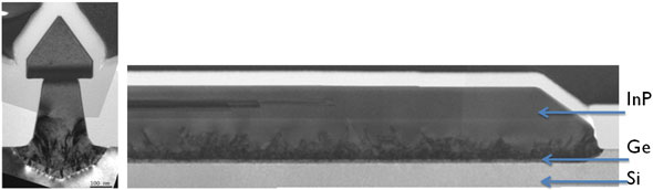
(Nanowerk News) Imec has demonstrated the selective area growth of high-quality InP layers on 200mm Si(001) wafers. Key to avoiding the typically formed and unwanted antiphase boundaries (APBs) is the creation of atomic steps on a thin Ge buffer layer. This result is a major step forward towards the fabrication of high-performance Ge/III-V CMOS devices and the integration of optoelectronic devices on a Si chip.
|
 |
| High-quality InP grown in shallow trench isolation (STI) trenches on Si(001) substrates.
|
|
APBs are typically induced by the reduced symmetry of III-V compounds when grown epitaxially on Si(001) or Ge(001). APBs cause deep levels in the band gap and therefore prevent further III-V-based device fabrication.
|
|
APBs are formed either in {111} or in {110} planes. The APBs in {111} may get annihilated with increasing layer thickness while the APBs in {110} will penetrate to the surface. To avoid APBs, miscut Si (001) or Ge (001) substrates are commonly used. These off-oriented substrates provide a high density of atomic steps that form double atomic steps at elevated temperatures, preventing APB formation. However, miscut substrates induce additional issues, especially in selective area growth, such as crystal quality and surface morphology dependence on pattern orientations, resulting in a significant barrier for their application in device fabrication. Consequently, it is of great importance to obtain APB-lean III-V layers on (001) oriented Si substrates.
|
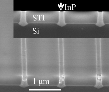 |
| Chemical-mechanical polished (CMPed) flat InP layers selectively grown in STI trenches on 200 mm Si(001) substrates.
|
|
Imec strongly suppresses the APBs by artificially creating double atomic steps on a rounded thin (<50nm) Ge buffer layer. The steps were created in a controlled way by annealing the Ge surface at a temperature above the Ge surface roughening point. By using this intermediate step, high-quality InP layers could be grown by selective area growth in submicron trenches on (001) oriented Si substrates. This approach solves the long-standing issue regarding APB formation of III-V epitaxial layers on standard (001) elementary semiconductor substrates.
|
|
The resulting APB-lean top InP layers provide the starting template for fabricating III-V devices on Si. The work also gives insight into the selective area growth of other III-V zinc blende compound semiconductor on Si(001) substrates. High-mobility channel materials such as III-V compound semiconductors are considered as cadidates for further boosting CMOS device performance. In addition, the integration of opoelectronic devices on a Si chip will also likely need selective area growth of III-V materials on dedicated Si areas.
|
|
This work has been published in Applied Physics Letters (G. Wang, et. al., Appl. Phys. Lett., 97, 121913 (2010)) and in the Journal of The Electrochemical Society (G. Wang et al., Journal of the Electrochemical Society, 157 (11), H1023-H1028 (2010)).
|