| Jan 20, 2011 | |
Simple, ingenious way to create lab-on-a-chip devices could become a model for teaching and research |
|
| (Nanowerk News) With little more than a conventional photocopier and transparency film, anyone can build a functional microfluidic chip. | |
| A local Cambridge high school physics teacher invented the process; now, thanks to a new undergraduate teaching lab at Harvard's School of Engineering and Applied Sciences (SEAS), students will be able explore microfluidics and its applications. | |
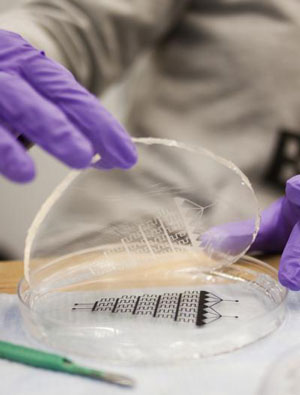 A student in the new Microfluidics Lab peels back the polymer, showing engraved channels, from an ink-transparency template. The Microfluidics Lab, developed by Dr. Anas Chalah, Director of Instructional Technology at SEAS, takes advantage of a simple but ingenious new method of creating lab-on-a-chip devices that are quick to produce, affordable, and reusable. Chalah is excited—contagiously so—about the lab's potential to serve students from all areas of science and engineering. "Harvard University shaped the emergence of the field of microfluidics and soft lithography through the leading research conducted in the labs of George Whitesides and David Weitz, among others," he says. "Now we are bringing those areas of experimentation to the undergraduate teaching labs at SEAS." The first course to use the lab will be the mechanical engineering course ES 123, "Introduction to Fluid Mechanics and Transport Processes." Students enrolled in the course this spring will use sophisticated COMSOL MultiphysicsTM software to model the flow of liquid through chips of varying structure, in order to design and build optimal chips in the lab. The COMSOL software is widely used for design projects in both academic research and industry. ES 123 is structured to emphasize the importance of the design process. "Students do the simulation, go through the homework, and get exposed to the process before they even get in the lab," says Chalah. Chalah emphasizes that the new lab will provide a core facility for multiple areas of undergraduate study. "We can get people from different disciplines excited about the same device," he says. |
|
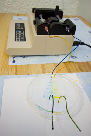 To demonstrate this concentration gradient generator, created in the lab at SEAS, two dyes are injected at the top, and they travel through a maze of tiny channels. The configuration of the channels, the flow rate of the dyes, and the material properties of the chip all affect the amount of mixing that can take place. At the end of the maze, a predictable concentration gradient is produced. For example, the do-it-yourself opportunity will also appeal to budding biomedical engineers and premedical students, who can use the lab-on-a-chip devices to study and test clinical applications. Chalah is particularly interested in a device called a concentration gradient generator, which allows two or more fluids to mix in a very controlled manner, producing a range of concentrations from 0 to 100 percent. A variation of the device is used in drug testing, as it can be used to deliver a range of very precise drug concentrations to a set of experimental cell lines. With multiple cell lines built into one chip, as many as 80 tiny experiments can be performed at once, all under the same controlled conditions. Chalah expects that bioengineering lab courses at SEAS will soon be developed that incorporate this technology. The technology used in the lab is not new, but a process that makes it affordable certainly is. Commercially available microfluidic devices (see image below) are produced in a clean room using high-resolution photolithography and etching, a process which pushes the retail price to around $500 each. Local high school physics teacher Joe Childs had a better idea: design the layout of the channels in PowerPointTM, print the image, and photocopy it onto a classroom-style transparency film several times until the layers of ink create raised ridges. The process results in a negative mold that can then be used to create channels in the polymer chip (see sidebar at top of page). It sounds rudimentary, but it works. |
|
| Childs, who teaches at the nearby Cambridge Rindge and Latin School, collaborates with faculty and students at SEAS through the Research Experience for Teachers (RET) program funded by the National Science Foundation's National Nanotechnology Infrastructure Network. | |
| He first developed the process in the lab of Bob M. Westervelt, Mallinckrodt Professor of Applied Physics at SEAS and Professor of Physics, with graduate student Keith Brown. He is now perfecting it with Chalah and an enthusiastic team of young interns for the undergraduate teaching labs. | |
| Together, they can design and build a chip in a single afternoon, and, Childs adds, "the most expensive thing that we need is a copy machine." | |
| The resulting chips are not as precise as the commercially available versions, but the benefit—besides the low cost—is that students will be able to experience the process of designing and building the devices themselves, applying their knowledge of the fundamental principles of fluid dynamics to create a functional tool. | |
| The simplified process will allow other science teachers to introduce their students to an aspect of physics that might previously have been off limits due to cost. | |
| "Believe me," says Chalah, "if people knew we could build a chip so cheaply, they would jump on it like this." | |
| The creation of the new Microfluidics Lab, on the ground floor of Pierce Hall, was enabled by a generous donation from Warren Wilkinson '41. The lab features state-of-the-art microfluidic pumps, microscopes, ovens, and soft lithography and fabrication equipment. |
| Source: Harvard University |