| Mar 22, 2011 |
The 'coolest' semiconductor nanowires
|
|
(Nanowerk News) Semiconductor nanowires are essential materials in the development of cheaper and more efficient solar cells, as well as batteries with higher storage capacity. Moreover, they are important building blocks in nanoelectronics. However, manufacturing semiconductor nanowires on an industrial scale is very expensive. The main reason for this is the high temperatures at which they are produced (600-900 °Celsius), as well as the use of expensive catalysts, such as gold.
|
|
Scientists at the Max Planck Institute for Intelligent Systems in Stuttgart, formerly the Max Planck Institute for Metals Research, have now been able to produce crystalline semiconductor nanowires at a much lower temperature (150 °Celsius) while using inexpensive catalysts, such as aluminium (Publication: "Metal-Catalyzed Growth of Semiconductor Nanostructures Without Solubility and Diffusivity Constraints"). In this way, nanostructured semiconductors can even be deposited directly on heat-sensitive plastic substrates.
|
|
Nanowires made of semiconductors such as silicon (Si) or germanium (Ge) will be indispensable for many technical applications in the future. Until now, they have been manufactured using a process that was first described in 1964. The so-called vapour-liquid-solid (VLS) mechanism utilises tiny particles of metal catalysts as seeds for the growth of the nanowires. The metal seeds are deposited on a solid substrate, melted and exposed to a gas atmosphere containing silicon or germanium. The metal droplets will then take up semiconductor atoms from the gas until they are supersaturated, and the excess semiconductor material precipitates at the boundary with the substrate: a nanowire grows. In most cases, gold is used as a catalyst, since it can dissolve a lot of silicon or germanium when molten. The use of this expensive catalyst and the high processing temperature of 600 to 900 ºCelsius lead, however, to high production costs.
|
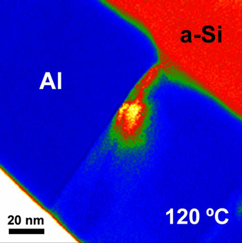 |
| Transmission electron micrograph of a cross-section of an aluminium-silicon bilayer during annealing. The image shows that the silicon flows into the spaces between the adjacent aluminium crystals (red: silicon; blue: aluminium) already at the low temperature of 120 °Celsius.
|
|
Materials scientists from Eric Mittemeijer's department at the Max Planck Institute for Intelligent Systems have now discovered a method to produce semiconductor nanowires at a strikingly lower temperature of only 150 °Celsius, while using cheap catalysts like aluminium. Together with colleagues from the Stuttgart Center for Electron Microscopy, a research facility at the same Institute, the scientists have managed to observe nanowire growth at an atomic scale in real time.
|
|
To this end, the scientists prepared a bilayer of crystalline aluminium and amorphous silicon. The layer was produced in vacuum and at room temperature using thermal evaporation. Whereas the atoms are disordered in the amorphous silicon phase, they are arranged in an ordered crystalline lattice in the aluminium layer. In fact, the Al layer is constituted of billions of tiny aluminium crystals, each of them of size as small as about 50 nanometres. The crystal grains are in tight contact with each other. Their boundaries thus form a two-dimensional grain-boundary network within the aluminium layer.
|
|
Using analytical transmission electron microscopy, the scientists were able to directly observe that silicon atoms begin to flow from the silicon layer into the aluminium catalyst at a temperature as low as 120 °Celsius. At such low temperatures, the aluminium catalyst is solid and cannot dissolve any silicon atoms. Microscopic investigations reveal that the silicon atoms are instead accommodated at the boundaries between the aluminium crystals. As more and more silicon atoms gather at the aluminium grain boundaries, they are restructured into tiny crystalline nanowires, as this reduces the total energy of the system. This produces a network of crystalline nanowires, the pattern of which is precisely determined by the aluminium grain-boundary network. Wires as thin as 15 nanometres can thus be produced.
|
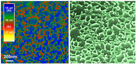 |
| Transmission electron micrograph (plan view) showing the formation of a silicon nanowire structure along the boundaries between adjacent aluminium crystals at 170 °Celsius (red: silicon; blue/green: aluminium). Right: Scanning electron microscope image (at a tilt angle of 30 degree) which shows the silicon nanowire pattern after removal of the aluminium by chemical etching.
|
|
Clearly the growth mechanism of nanowires discovered by the material scientists in Stuttgart is fundamentally different from the conventional VLS growth mechanism. Most strikingly, the new growth method does not require semiconductor solubility in the metal catalyst and can therefore be realized at low temperatures (150 °Celsius), while using cheap catalysts like aluminium.
|
|
The major benefits of the new method are therefore that it does not require high substrate temperatures or expensive catalysts. In addition, materials scientists can tailor the size of the aluminium grains and thereby the form of the aluminium grain-boundary network, to produce the desired pattern of silicon nanowires. The Al catalyst can easily be removed through selective etching. Since aluminium films have been used in microelectronics for decades, their production and processing are widely established. Other catalysts may also be suitable for the method. Another advantage is that nanostructured silicon devices can be grown directly on most plastic substrates, even if they are heat-sensitive.
|