| Apr 18, 2011 |
Polysterene spheres self-assembled onto graphene can be used to pattern ribbons and other shapes
|
|
(Nanowerk News) Since graphene was first isolated as single atomic layers in 2004, researchers have increasingly focused on reducing its size in the lateral dimension. Sheets of graphene are useful in many situations for their lack of an energy barrier, or bandgap, to prevent electrons from moving freely. For electronic devices such as transistors, however, a bandgap and the corresponding semiconducting behavior are essential, and narrow ribbons of graphene are known to display this property.
|
|
Enge Wang, Wenlong Wang and colleagues at the Beijing National Laboratory for Condensed Matter Physics and Peking University in China have now reported a simple and scalable method for manufacturing such graphene nanoribbons ("Nanosphere Lithography for the Fabrication of Ultranarrow Graphene Nanoribbons and On-Chip Bandgap Tuning of Graphene").
|
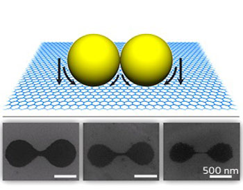 |
| Schematic diagram (top) showing the sphere-based etching of graphene sheets into dumbbell-like graphene structures (bottom, electron microscopy images) with nanoribbons that become narrower with etching time.
|
|
The researchers prepared their graphene ribbons by covering a sheet of graphene with 1 µm polysterene spheres, which self-assembled on the surface into tightly packed arrays, and then etching the sample with oxygen plasma. Due to the distribution of plasma ions between the spheres, the etching process patterned the graphene into complex shapes including dumbbells (see image), branched networks of ribbons, linear and circular chains, and polygonal rings, which could be recovered easily after washing away the spheres. The researchers could produce specific patterns by controlling the etching time and the sphere packing geometry.
|
|
Crucially, the narrow graphene ribbons prepared using this technique exhibit a bandgap, which could make them useful in electronic components such as transistors. Wang and his colleagues demonstrated this utility by constructing a transistor from a graphene sheet and then gradually etching the graphene using their polystyrene bead-based process. The transistor, which did not display transistor function before etching, showed good transistor functionality after etching for just 30 seconds, achieving an on–off ratio of 90 for current switching. The conductivity of the graphene transistor channel was reduced by a factor of about 1,000 times by the etching process.
|
|
The fabrication technique is relatively simple and inexpensive, is capable of forming many graphene nanoribbons at the same time, and can even be used to modify finished devices. Future work will include research to understand the effects of the etching process on the ribbon edges, where atomic disorder can strongly affect the device's electrical properties.
|