| May 23, 2011 |
Large two-dimensional molecular crystals promising for organic electronics
|
|
(Nanowerk News) One of the most striking properties of graphene is arguably its two-dimensionality. The remarkable electronic behavior realized by this two-dimensionality has prompted researchers to try and form similar two-dimensional sheets from other materials. Wenping Hu and colleagues from the Beijing National Laboratory for Molecular Sciences in China have now succeeded in growing two-dimensional crystals of an organic semiconductor on large scales and on various types of substrate with a view to developing advanced organic electronic devices ("Millimeter-Sized Molecular Monolayer Two-Dimensional Crystals").
|
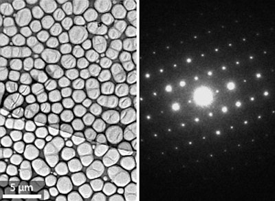 |
| Transmission electron microscopy image of the two-dimensional organic crystal (left), and the corresponding selected-area electron diffraction image (right) showing the excellent crystallinity. (© 2011 Wiley-VCH)
|
|
The researchers were able to prepare two-dimensional crystalline films of the organic molecule HTEB by casting from a chlorobenzene solution onto silicon, SiO2, quartz and other amorphous substrates. After evaporation of the solvent, they observed the formation of microcrystals filling an area on the millimeter scale (see image). The thickness of the crystals could be changed by varying the concentration of the solution. After optimization of the preparation conditions, the team confirmed the formation of film just 3.5 nm thick — equivalent to a single layer of molecules.
|
|
To test the utility of the monolayer crystals in electronics applications, the researchers developed the films as part of organic field effect transistors (OFETs). The mobility of the monolayer-based OFETs was comparable with that of transistors based on amorphous silicon, confirming the excellent electronic performance of the monolayers. In addition, the team observed that there was no clear dependence of mobility on film thickness, further evidence that the electronic transport occurs primarily at the interface with the substrate as expected.
|
|
The OFETs of the molecular monolayer crystals exhibited excellent stability, which, combined with the facile solution process and the high mobility of the crystals, demonstrates the strong potential of the two-dimensional crystals for applications in organic circuits.
|
|
According to Hu, the results provide direct proof of an important and fundamental challenge in organic electronics — understanding the minimum functional thickness of an organic semiconductor for use as an ideal channel in an OFET, and clarifying the correlation between the minimum thickness of the conducting channel and that of other layers of the active semiconductor. To demonstrate the advantages of the synthesized materials, the team is now aiming to fabricate organic electronic circuits based on their two-dimensional crystals.
|