| Jun 06, 2011 |
Graphene nanoribbons: Drawn together
|
|
(Nanowerk News) Graphene exhibits a suite of unusual electronic properties, among which is its very high electron mobility. This has attracted the attention of researchers and technologists alike for realizing fast and efficient electronic devices. One problem with large sheets of graphene, however, is that in this form graphene does not behave as a semiconductor, meaning that is difficult to control its electronic properties with external fields — an essential functionality for device applications.
|
|
One way around the problem is to use graphene nanoribbons — narrow strips of graphene that retain the material's high mobility but which behave like a semiconductor. Nanoribbons have other problems though: the mobility is severely degraded if the ribbon edges are rough and if the substrate used is not flat, and it is difficult to fabricate nanoribbons with reproducible size and properties, making scalability an issue.
|
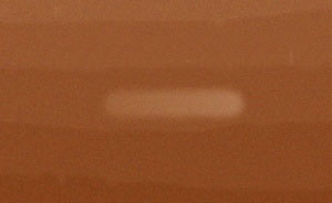 |
| An atomic force microscopy image of a nanoribbon (~100 nm long) drawn by dip-pen nanolithography.
|
|
Jong Yeog Son from the Pohang University of Science and Technology in Korea and colleagues have now developed a technique that allows for the scalable production of nanoribbons and demonstrated their use in high-mobility field-effect transistors ("High-Mobility Graphene Nanoribbons Prepared Using Polystyrene Dip-Pen Nanolithography").
|
|
The researchers deposited large flakes of exfoliated graphite on a strontium titanate (SrTiO3) film grown on a niobium-doped SrTiO3 substrate. The advantage of using SrTiO3 is twofold: it can be etched in a solution to give an atomically flat surface, and it has a high dielectric constant, which is essential for use in field-effect transistors. "The choice of a dielectric material with high dielectric constant is crucial to produce properties such as the required gate response in graphene nanoribbon-based transistors," says Son.
|
|
The nanoribbons were then 'drawn' in the graphene using a technique called 'dip-pen nanolithography', in which the tip of an atomic force microscope is used to transfer organic molecules onto a substrate in a controlled way. Son and his colleagues used this method to lay polystyrene nanorods on top of the graphene surface. They then etched the surface using oxygen plasma, leaving only graphene nanoribbons on an atomically flat, high-dielectric-constant substrate (see image).
|
|
The team succeeded in depositing source and drain contacts on the nanoribbons to form field-effect resistors, obtaining an average room-temperature mobility 2–3 times higher than of previous devices.
|