| Jun 16, 2011 |
Procedure for carrier profiling in nanowire-based transistors
|
|
(Nanowerk News) Semiconductor nanowires are one of the most promising building blocks for future nanoelectronic devices such as transistors, sensors and solar cells. Nanowire-based tunnel field-effect transistors (TFETs), for example, are widely seen as potential successors of standard MOSFETs, due to the absence of a 60mV/dec sub-threshold swing limitation and reduced short-channel effects.
|
|
But to optimize the fabrication processes for such high-performance devices, it is necessary to have a thorough understanding of the active dopant (carrier) distribution. Therefore, researchers from imec have recently extended the applicability of HV-SSRM as a metrology tool for carrier mapping to fully integrated nanowire-based transistors ("Observation of diameter dependent carrier distribution in nanowire-based transistors").
|
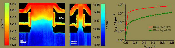 |
| Quantitative 2D-carrier distribution for nanowire diameters of 400nm and 100nm. The difference in drain doping is reflected in the TFET off current.
|
|
Applying HV-SSRM to Si-nanowire-based tunnel-FETs, the team identified a diameter-dependent dopant-deactivation mechanism. This mechanism occurs in small 3D structures only and cannot be predicted using standard process simulation tools. It could be shown experimentally and through device simulations that this phenomenon directly impacts the device characteristics. The validity of the technique is proved by the observance of the diameter dependency of the carrier distribution in the nanowire top-section. This results from a tilted ion implantation step and is perfectly in agreement with results from process simulations.
|
|
Scanning spreading resistance microscopy (SSRM) is a technique with a unique combination of high spatial resolution (1 to 3nm) and high sensitivity. SSRM is based on atomic force microscopy and was invented by W. Vandervorst et al. at imec in 1994. During the last decade, it has evolved into the method of choice for carrier profiling in planar MOS transistors. With this work, imec applied HV-SSRM to Si-nanowire-based tunnel-FETs, proving its validity to study carrier distribution in semiconductor nanowires. It also showed that HV-SSRM is capable of revealing physical phenomena which are present in small, 3D structures only, and which cannot be predicted by blanket experiments. Such information is essential for the process development of future nanowire-based devices.
|