| Jun 22, 2011 |
Faster simulation brings nanoscale optical surface characterization closer to practical reality
|
|
(Nanowerk News) The roughness of a surface can make all the difference in nanoscale devices. Measuring the roughness of such delicate surfaces in the hard-to-reach places of nanodevices, however, is no easy task. The ideal surface measurement technique should avoid any physical contact with the sample. Vertical scanning interferometry is a well-established zero-contact surface characterization technique, but the analysis involved in interpreting the data is complex and computationally intensive. Wee Keat Chong at the A*STAR Singapore Institute of Manufacturing Technology and co-workers have now developed a computationally efficient model for this technique ("Computationally efficient signal modeling for vertical scanning interferometry").
|
|
Vertical scanning interferometry involves illuminating an unknown surface of interest, and also a known reference surface, with two separate beams of light that have been split out from a single source. The beams reflected from the two surfaces are then made to meet, creating an interference pattern called an interferogram (pictured). By analyzing the interferogram while one of the surfaces is moved, which changes the optical path difference between the surfaces, the unknown surface can be characterized with nanoscale resolution.
|
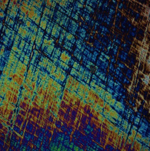 |
| An interferogram showing the difference in surface height between a reference and a sample surface.
|
|
To deal with experimental errors, researchers rely on simulation models. The most accurate model is based on numerical integration, which is a computationally intensive problem that requires considerable time to complete. While simplified models exist, they tend to rely on parameters that cannot be derived directly from knowledge of the experimental setup, reducing their predictive power and accuracy. Chong and co-workers succeeded in developing an alternative simplified model with well-understood and physically based parameters.
|
|
They did this by introducing an approximate mathematical representation of the spectrum of the light source used for interferometry measurements. Numerical integration is generally used to model this spectrum through the summation of one or more Gaussian functions. Instead of using the full Gaussian mathematical form, the researchers represented each Gaussian as a sum of two piecewise cosine functions, allowing the interference signal to be simulated without any numerical integration.
|
|
As a result, the interference signal from a vertical scanning interferometry measurement could be simulated over 200,000 times faster than through the use of direct numerical integration. The development of such a simplified model is timely given the increasing use of white light emitting diodes (LEDs) as the light source in optical measurement technologies. "The spectrum of white LEDs could vary tremendously from product to product, so a computationally efficient model of interferometry using an arbitrary light spectrum should prove to be quite valuable," says Chong.
|