| Jun 27, 2011 | ||
Hands-on courses prepare students for careers in nanotechnology |
||
| (Nanowerk News) Two million workers are projected to be needed in nanotechnology-based businesses by 2020 in the United States alone. Today, demand far outstrips the availability of trained personnel and the College of Engineering and Applied Science is seeking to meet this need with courses developed and implemented in conjunction with University of Cincinnati's (UC) Nanoworld Laboratory. | ||
| Two new cross-disciplinary courses — "Nanoscale Devices" and "Environmental Aspects of Nanotechnology" — developed through undergraduate education research at the University of Cincinnati provide hands-on experimental modules that help meet the growing demand for nanotechnology education in institutions of higher learning. | ||
| Because nanotechnology involves a much more intricate level of investigation than traditional research, students must use new approaches and develop precise skills. Skills that require hands-on experience with advanced tools such as robots, manipulators and probes are a staple for this instruction. Four modules addressing design, construction, and emerging application of nanoscale devices were developed as part of the "Nanoscale Devices" course. Three additional modules were needed for the new "Environmental Aspects of Nanotechnology" course which covers environmental applications and the environmental impact of nanotechnology. | ||
| The new courses build on the background that students gain in their existing courses titled "Introduction to Nanoscale Science" and "Technology and Experimental Nanoscale Science and Technology." Students at UC have an outstanding educational advantage in nanoscale science and engineering. All four courses are offered yearly and form the basis for a minor in interdisciplinary nanoscale science and technology. The courses are cross-listed by the UC Colleges of Engineering and Applied Science and McMicken College of Arts and Sciences, making them readily available to students in many different scientific disciplines in addition to engineering and technology. | ||
| Eight students took "Nanoscale Devices" during its initial offering in the fall of 2010-11, and the course was rated very highly. Students felt it contributed to development of their professional skills in designing and conducting experiments, using techniques, skills and understanding modern engineering tools. One student said, "Hands-on learning by means of experimentation helped provide insight in the direction of research." Students will take "Environmental Aspects of Nanotechnology" during winter quarter of the 2011-12. | ||
| UC doctoral student Christopher Huth is presenting research on engineering education detailing the development of hands-on experimental modules for integration into undergraduate courses in nanotechnology at the 2011 Annual Conference of the American Society for Engineering Education (ASEE). The conference is in Vancouver, BC, on June 26-29, 2011. Huth is part of an investigative team that includes F. James Boerio, Dionysios D. Dionysiou, Ian Papautsky, Miguel Pelaez, Mark Schulz, Vesselin N. Shanov, and Donglu Shi. | ||
 |
||
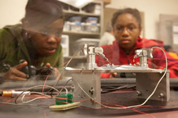
| (L to R) Nykaila Taylor and Hadiya Harrigan, two students from the 2010 CEAS Summer Institute, learn to use joysticks to control a nanomanipulator measuring resistance in a carbon nanotube thread. | ||
| Huth is also reporting on successful efforts to adapt the experimental modules for presentation to students during the Summer Institute conducted by CEAS as part of an outreach program in summer 2010. The college's Summer Institute is a five-week program designed to increase awareness and interest in STEM fields. The program targets ethnic students from high schools and junior high schools throughout the greater Cincinnati area. | ||
| Nanoscale: An underworld of discovery and promise | ||
| Considering a grain of sand ranges from 2 mm to .05 mm in diameter — equivalent to 2,000,000 to 50,000 nanometers — the nanoscale level represents somewhat of an underworld in which developments occur well under the ability for detection by the naked eye and many microscopes. Nanoscale materials are considered particles or other shapes having one dimension or more in the range of 1 to 100 nanometers. This is roughly one millionth of the width of a human hair. | ||
| It has only been in the last 30 years with the development of the scanning tunneling microscope (STM) and atomic force microscope (AFM) that scientists have been able to gain entry into viewing and manipulating particles at the molecular and atomic level. These two important investigative tools have allowed scientists to study and work in the nanoscale. Researchers can now understand and utilize the unique physical, chemical, mechanical, and optical properties of materials that naturally occur in nanoscale. | ||
| Early work in nanoscience revealed that almost all solid matter has new or different properties at the nanoscale compared to bulk materials. At dimensions of about 1–100 nanometers, the behavior and properties of particles are dictated by quantum and surface effects that are size-dependent. According to Professor Vesselin Shanov of UC Nanoworld Laboratory: "These properties depend on the composition, size, and shape of the material… This has opened up a whole new world of discovery for scientists and a transforming world of applications for engineers." | ||
| Some of the properties that may change at nanoscale include high specific strength and modulus, high electrical and thermal conductivity, large surface area to volume ratios, nearly defect-free structure, and more concentrated sensing and actuation properties. | ||
 |
||
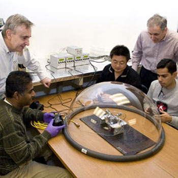
| (Seated: L to R) Doctoral students Chiaminda Jayasinge, Weifeng Li and Pravahan Salunke demonstrate a new nanomanipulator that will be used for tasks in the vacuum environment of a scanning electron microscope (SEM) as Shanov and Schultz (standing) observe. | ||
| Shanov and Professor Mark Schulz are co-directors of UC Nanoworld Laboratory, which specializes in the fabrication of high quality carbon nanotubes (CNT). The thrust of Nanoworld's research is to introduce innovations in fabrication of high quality CNT arrays, and to process them into CNT materials that can become electrical wires for power distribution or electronic and biomedical devices. UC Nanoworld provided the facility and expertise for students in the development of the experimental modules by Huth and the investigation team. | ||
| Nanotechnology: The sky is no longer the limit! | ||
| Imagine a lightweight carbon nanocomposite airplane that detects structural damages and assures safety during flight… Or solar stations orbiting the globe transferring clean energy to earth through carbon nanotube electrical fibers… Or leaving the planet by a space elevator climbing a nanotube ribbon beyond the atmosphere to an orbiting space station. | ||
| In medicine nanoparticles may precisely target cancer cells and deliver anti-cancer toxin to eradicate tumors without destroying surrounding tissue while a CNT ribbon scaffold promotes repair of damaged nerve tissue and overcomes paralysis. And there is more - nanoparticles may be used to do environmental remediation of tainted ground water by seeking out and reacting with pollutants and cloth from CNT threads is being made into protective coats for firefighters that are both light weight and fire resistant. | ||
|
While these applications are evolving, there are already some 800 commercial products using nanomaterials. To name just a few: nanoparticles added to polymer composites provide durability and resiliency in baseball bats, tennis rackets, and motorcycle helmets; nanotechnology used in batteries makes them less flammable, more efficient and lighter; and many new televisions and laptop computer displays use organic light-emitting diodes (OLED) with nanostructured polymer films. According a study** by National Center for Manufacturing Sciences (NCMS) sponsored by the National Science Foundation (NSF): "Nanotechnology is no longer a technology in waiting - a great breadth and diversity of nanotechnology products and application markets are being pursued with the potential for disruptive economic, social, environmental and military advantage." As nanotechnology becomes more commonplace, courses made available at the University of Cincinnati featuring modules developed through this research will continue to be leading edge and will prepare a new generation of scientists and engineers for nanotechnology. Research support for this engineering education investigation project is provided through a $200,000 grant (EEC-0939320) entitled "NUE: Integration of Nanoscale Devices and Environmental Aspects of Nanotechnology into Undergraduate Engineering and Science Curricula" from the National Science Foundation's Nanotechnology in Undergraduate Education (NUE) program at the University of Cincinnati (UC) under the direction of Principal Investigator F. James Boerio. Co-Principal Investigators include Anant Kukreti, Donglu Shi, Dionysios Dionysiou and Vesselin Shanov. |
||
| Modules developed for the course Nanoscale Devices are "Introduction to Carbon Nanotube applications, "Synthesis of Nanoparticles as Sensor Building Blocks," "Making Wireless Biosensors Using a Nanomanipulator" and "Electrochemical Sensors in Fluidic Channels." | ||
| Modules developed for the new course Environmental Aspects of Nanotechnology are "Magnetic Separation of Toxins by Applied Fields," "Magnetic Measurement of Nanoparticles" and "Active Nanosystems for the Destruction of Toxins in Water." | ||
| The new and existing courses also support UC students participating in the Engineering Research Center (ERC) for Revolutionizing Metallic Biomaterials in which UC partners with lead institution North Carolina Agricultural and Technical State University and the University of Pittsburgh. | ||
| CNTs and UC Nanoworld Laboratory – Research Holds Great Promise | ||
| UC's Nanoworld Laboratory currently produces the longest carbon nanotube arrays in the world. UC Nanoworld is comprised of three separate laboratories. The Nanotube Synthesis Laboratory for carbon nanotube production and the Nanostructured Materials Processing Laboratory is where nanomaterials are modified and incorporated into other materials such as polymer nanocomposites. The Smart Materials and Devices Laboratory is where nanomaterials are manipulated, assembled and processed into sensors, actuators and devices which are then evaluated for practical applications. | ||
| Carbon nanotubes are central to many of the developing applications in nanotechnology. A breakthrough application of UC nanotubes is to spin thread. Long carbon nanotubes (CNT) called "Black CottonTM" are used to spin thread to provide lightweight reinforcement, sensing, and actuation simultaneously. An application example uses carbon nanotube thread/cloth to reinforce spacecraft and space structures and to build a prototype ribbon material for a space elevator. These structures evaluate and monitor their own health through the conductive properties of the carbon thread. | ||
| The CNT thread could become a preferred alternative to copper wires. Conductivity is so good that a tiny CNT light source may be capable of emitting light at levels rivaling that of existing incandescent or fluorescent bulbs while consuming substantially less power. | ||
| Source: By Tom Curtis, University of Cincinnati |