| Jul 04, 2011 |
Silicon nanowires: Bent to disorder
|
|
(Nanowerk News) Semiconductor nanowires could form the basis of future nano-scale electronic components such as transistors, actuators or even power sources. In developing such technologies, it is important to assess how the nanowires might perform under stress in real devices.
|
|
Xiaodong Han and co-workers from the Beijing University of Technology and Zhejiang University in China have now discovered that when silicon nanowires are bent, they undergo a dramatic transformation from an ordered crystal structure to a completely disordered, or 'amorphous', state ("Direct Atomic-Scale Imaging about the Mechanisms of Ultralarge Bent Straining in Si Nanowires").
|
|
The researchers were inspired by previous experiments in which the probe tip of an atomic force microscope was used to bend single silicon nanowires. Those studies indicated that nanowires can withstand high tensile and elastic strains, but no-one had yet identified the changes that occur in the atomic structure of the nanowire under such extreme conditions.
|
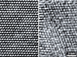 |
| Transmission electron microscopy images showing the atomic structure of silicon nanowires before (left) and after (right) bending.
|
|
Han and his co-workers took a new approach that involved scattering nanowires onto a colloidal film with a hair-like surface coating. They then irradiated the area with an electron beam, which caused the film to shrink and many of the nanowires to be bent into extreme shapes. "Individual nanowires can be held by the 'hands' of the colloidal film so that the bending strain of individual nanowires can be directly observed at an atomic scale," explains Han.
|
|
As the researchers examined transmission electron microscopy images of the bent nanowires (see image), they noticed the appearance of dislocations in the crystal lattice as the strain increased. They also found that the dislocations were mobile, propagating through the nanowire crystal to produce more dislocations. At high strain, the dislocations took on a 'Lomer lock' structure, which cannot be easily reversed. Eventually, the crystal structure was lost entirely, resulting in a nanowire with an amorphous atomic structure.
|
|
This discovery could explain why many other semiconductor nanostructures, such as boron carbide or germanium nanowires, or silicon nanobeams can be deformed to a great extent. However, Han believes that the shift towards an amorphous atomic structure could lead to some significant changes in nanowire function. "Due to the disordered nature of the amorphous state, many atoms have unsaturated chemical bonds, which can cause anomalous electrical behaviors," he says. "The knowledge we gained in this study is highly valuable for developing flexible electronics using nanowires."
|