| Jul 04, 2011 |
Position control of a transistor source-drain junction with sub-nanometer accuracy
|
|
(Nanowerk News) Wataru Mizubayashi, Shinji Migita, Hiroyuki Ota, and Meishoku Masahara of the Si Nano-Devices Group, the Nanoelectronics Research Institute of the National Institute of Advanced Industrial Science and Technology (AIST), have developed a new metal source–drain junction technology that can be applied to the transistors of 16-nm generation and beyond.
|
|
In the very small metal-oxide-semiconductor (MOS) transistors of 16-nm generation and beyond, the parasitic resistance of the source–drain junction will become a big issue because it would ruin an improvement of the transistor performance. In addition, it is a big challenge to fabricate a source–drain junction accurately in transistors with a gate length in the order of 10 nm. The developed technology allows us to control the position of a very low-resistive metal source–drain junction at the sub-nanometer level. The control technology has been demonstrated to increase transistor performance significantly and should provide a solution to junction position control in the MOS transistors of 16-nm generation and beyond. This research and development project was carried out under the Next-generation Semiconductor Materials and Process Technology (MIRAI) Project commissioned by the New Energy and Industrial Technology Development Organization (NEDO).
|
|
Details of this technology has been presented at the 2011 Symposium on VLSI Technology to be held in Kyoto from June 14 to 16, 2011.
|
|
Social Background of Research
|
|
The performance and density of silicon integrated circuits have been improved by miniaturizing transistor devices, the smallest components of silicon integrated circuits. Because miniaturization of transistor devices leads to cost reduction, fierce competition continues in the development of nano-devices. The transistors of 16-nm generation are thought to be introduced into the market in 2016 or later. The biggest challenges in developing transistor technologies for 16-nm generation and beyond are to reduce the parasitic resistance around the source–drain junction in silicon semiconductors to which impurities such as phosphorus, arsenic, and boron have been added at high concentrations, and to develop a technology to accurately form source–drain junctions in transistors with gate lengths in the order of 10 nm. In particular, since fluctuation in a junction position causes a large variation in transistor characteristics, there is strong demand for the development of a technology to control junction positions at the nanometer level.
|
|
History of Research
|
|
AIST has developed advanced CMOS process technologies for the practical application of very small transistors as part of MIRAI Project commissioned by NEDO. In 2005, we developed a very low-resistive nickel disilicide (NiSi2) metal source–drain junction and confirmed that the resistance of this junction was 1/100 of that of conventional heavily-doped silicon semiconductor junctions. In 2010, we developed the world's thinnest high-permittivity gate insulating film with an equivalent silicon oxide thickness of 0.5 nm, and applied it to transistors. (AIST press release on December 8, 2010). We are also developing transistors using a silicon-on-insulator (SOI) substrate.
|
|
Details of Research
|
|
Figure 1 compares a conventional heavily-doped silicon semiconductor source–drain junction and the metal source–drain junction. The silicon semiconductor source–drain junction is formed by ion implantation of phosphorus, arsenic, boron, and other impurities and high-temperature heat treatment. This results in variation in junction characteristics owing to fluctuation in implantation positions and thermal diffusion, and an increase in resistance due to a decrease in the concentrations of the dopants (phosphorus, arsenic, boron, and other impurities) at the junction interface. On the other hand, the metal source–drain junction is fabricated at a relatively low temperature by a solid-state reaction of a metal and silicon. This eliminates the variation in junction positions and creates steep junction interfaces, making it possible to significantly reduce the variation in junction characteristics.
|
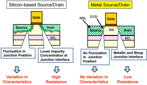 |
| Figure 1: Comparison between the silicon semiconductor source–drain junction and the metal source–drain junction.
|
|
A NiSi2 crystal tends to form a stable structure surrounded by (111) planes. We investigated the growth of a NiSi2 crystal formed in a very thin silicon layer to examine the possibility of controlling the position of the metal source–drain junction in a very small transistor. An 8-nm-thick SOI layer was prepared and a dummy gate-stack structure was formed. A nickel film was formed and then heat treated at 500 ºC to form a NiSi2 crystal. As the size of this crystal is nearly the same as that of a silicon crystal, the NiSi2 grows keeping an epitaxial structure. Unreacted nickel was removed and HfO2 films were deposited to make the initial reaction rims clear in cross-sectional observation by a transmission electron microscope (TEM).
|
|
Figure 2 shows cross-sectional TEM images of the change in positions of the epitaxial NiSi2 source–drain junctions with different heat treatment times. After 1 minute of heat treatment, the NiSi2 crystal had metastable (100) and stable (111) planes. After 100 minutes of heat treatment, the crystal had grown in <100> direction, reached the embedded SiO2 interface (BOX in the figure), and then stopped growing. The position of the (111) plane of NiSi2 remained unchanged. After 300 minutes of heat treatment, the NiSi2 crystal had grown laterally while maintaining the stable (111) plane. This growth corresponds to the change in the position of the transistor junction. The crystal grew laterally by 8 nm after the 300-minute heat treatment. In this phenomenon, the growth rate depends on the diffusion of atoms in the crystal, and therefore the extent of growth depends on the square root of the time. The growth rate was estimated to be 0.04 nm/min. Since the rate is very slow, the position of the junction can be controlled at the nanometer level.
|
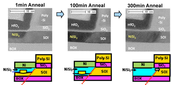 |
| Figure 2: Cross-sectional TEM images showing the change in the positions of the epitaxial NiSi2 source–drain junctions with different heat-treatment times. "BOX" in the figure denotes embedded SiO2 and "poly-Si" denotes polycrystalline silicon.
|
|
We fabricated transistors with the same gate-stack structure and gate length by changing only the heat treatment time, and we then assessed the effect of the junction positions on transistor characteristics. Figure 3 compares the characteristics of the transistors. The drain current increased by more than 20% when the junction positions were made closer. It was confirmed that the variation of the characteristics did not increase. This position control technology for the metal source–drain junction by utilizing the properties of NiSi2 crystal growth is expected to be a new junction technology for the MOS transistors of 16-nm generation and beyond.
|
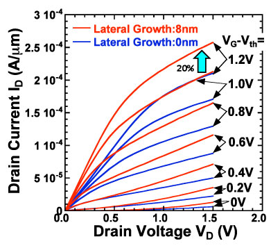 |
| Figure 3: Drain current–drain voltage (Id–Vd) characteristics of epitaxial NiSi2 source–drain junction MOS transistors with a gate length of 50 nm: performance comparison between a transistor subjected to 1-minute heat treatment (0 nm lateral growth) and that subjected to 300-minute heat treatment (8 nm lateral growth). The lateral growth of 8 nm meant that the effective gate length was reduced by 16 nm.
|
|
Future Plans
|
|
The developed technology will enable us to solve the increasing difficulties faced in improving transistor characteristics, particularly in the MOS transistors of 16-nm generation and beyond, and to further miniaturize MOS transistors. Our next goals are to develop further miniaturized transistors and to demonstrate performance improvement at the circuit level.
|