| Jul 11, 2011 |
Topological Insulators: Getting defects under control
|
|
(Nanowerk News) The study of how charge flows through two-dimensional surfaces has been one of the fastest growing areas of research in physics over the past decade. More recently, however, scientists have begun to focus on charge flow through the two-dimensional surfaces of three-dimensional objects called topological insulators. The surfaces of topological insulators exhibit unique electrical and magnetic properties that are not found in the bulk of the object.
|
|
A key challenge in topological insulator research is the large density of bulk states, which makes observing surface states difficult. Bismuth-based topological insulators, for example, have a high density of bulk electron donors. Researchers have succeeded in compensating for these donors by adding electron-accepting donor atoms like calcium or tin, but the heavy doping concentrations employed leads to charge scattering and low charge mobility. Qi-Kun Xue and colleagues from Tsinghua University and the Institute of Physics in China and Rensselaer Polytechnic Institute in the US have now succeeded in controlling charge densities in bismuth-based topological insulators without the use of any external doping ("Topological Insulator Thin Films of Bi2Te3 with Controlled Electronic Structure").
|
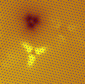 |
| A scanning tunneling microscopy image of two defects in a thin film of the topological insulator Bi2Te3. (© 2011 Wiley-VCH)
|
|
The researchers achieved this in thin films of the topological insulator Bi2Te3 by controlling film growth. They began with a standard fabrication approach called molecular beam epitaxy, in which they exposed a substrate to molecular beams containing bismuth and tellurium. By carefully tuning the ratio of the beam flux and the substrate temperature, they were able to control the density of defects in the growing film's crystal structure. Because defects can also act as charge donors and acceptors, this provided fine control over the film's charge density, which could be tuned from n-type (dominated by negative carriers), to insulating and p-type (dominated by positive carriers).
|
|
Critically, this control was possible with a defect concentration that was much lower than the concentration of extrinsic dopants (like added calcium atoms) that would be necessary to achieve the same effect. As a result, the work should enable researchers to observe the exotic physics associated with pure surface states in relatively pristine topological insulator materials. "If we can achieve bulk-insulating thin films or heterostructures by control of defects," says Xue, "we may eventually observe the quantum Hall effect and other novel topological phenomena."
|