| Aug 17, 2011 |
A one-pot synthesis provides a simpler and faster route to highly efficient solar cells
|
|
(Nanowerk News) Preventing the recombination of free charges produced when light strikes a solar cell is one of the main goal of engineers attempting to extract the maximum energy conversion efficiency from their devices. One way to achieve this is by building into the cell a 'heterojunction' between positive (p) and negative (n) type semiconductors, which allows the light-induced positive and negative charge to escape the cell by moving in opposite directions at the heterojunction interface.
|
|
Mingyong Han at the A*STAR Institute of Materials Research and Engineering and co-workers have now discovered a way to produce high-quality nanoscale heterojunctions, setting the stage for cheaper and more efficient photovoltaic devices ("One-Pot Synthesis of Cu1.94S-CdS and Cu1.94S-ZnxCd1-xS Nanodisk Heterostructures").
|
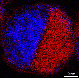 |
| Energy-filtered transmission electron microscopy image of a two-component hexagonal nanodisk showing the distributions of cadmium (blue) and copper (red). (© 2011 ACS)
|
|
Nanoscale semiconductor crystals provide enhanced surface area for light absorption and are also cheaper to produce than conventional lithography-patterned cell structures. However, it has been extremely difficult to form high-quality heterojunctions between n- and p-type semiconductors in a way that achieves the intimate inter-crystal contact needed to enhance device performance.
|
|
Resolving this problem requires a technique that can bind the two semiconductors together chemically. Previous studies have produced binary nanocrystals with a spherical 'core–shell' structure. Unfortunately, heterojunction based on these nanocrystals have low energy conversion efficiency because light has difficulty reaching the inner core. Han and his co-workers overcame this problem by adopting a different route for synthesis.
|
|
First, the researchers used a blend of surfactants under hot thermal conditions to produce copper(I) sulfide (CuxS), a well-known p-type semiconductor, in distinctively shaped hexagonal disks roughly 40 nanometers wide and 15 nanometers thick. The well-defined facets of these novel materials enabled the researchers to nucleate the crystallization of n-type cadmium sulfide (CdS) onto the outer edges of the crystals.
|
|
Next, through a process known as cation exchange, the researchers persuaded the n-type crystals to grow inward, effectively chemically converting a portion of the CuxS disks into CdS. "This method results in nano-heterostructures with the same morphology as the original material," says Han. By carefully optimizing the reaction conditions, the researchers transformed the hexagonal nanodisk into a perfectly symmetric, side-by-side heterojunction (see image). Zinc metals were also incorporated into the interface to further tweak its electrical performance.
|
|
Han notes that the CuxS–CdS heterostructure is promising for solar cell technology because of its dually accessible surface and an energy band alignment that drives strong charge separation. The team also expects to synthesize a wide range of new semiconductor pairs with this one-pot technique, taking advantage of the system's extraordinary crystallization properties.
|