| Aug 19, 2011 |
Nanoscientists invent better etching technique
|
|
(Nanowerk News) Imagine yourself nano-sized, standing on the edge of a soon-to-be computer chip. Down shoots a beam of electrons, carving precise topography that is then etched the depth of the Grand Canyon into the chip.
|
|
From the perspective of scientists at the U.S. Department of Energy's Argonne National Laboratory, this improved form of etching could open the door to new technologies.
|
|
Argonne nanoscientist Seth Darling and colleagues at Argonne's Center for Nanoscale Materials and Energy Systems Division say it has the potential to revolutionize how patterns are transferred onto different materials, paving a new approach for the next generation of energy, electronics and memory technologies.
|
|
The innovation combines new tricks with an old technology.
|
 |
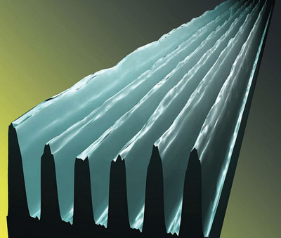
| Deep canyons can be etched into materials at the nanoscale with a new SIS-based lithography technique by Argonne National Laboratory scientists.
|
|
One of the biggest recent questions facing materials science has involved the development of better techniques for high-resolution lithographies such as electron-beam, or e-beam, lithography. E-beam lithography is used to manufacture the tiniest of structures, including microelectronics and advanced sensors; beams of electrons are part of a process that "prints" desired patterns into the substance.
|
|
Transferring patterns more deeply into materials would allow scientists to craft better electronics.
|
|
To create a pattern using e-beam lithography, researchers have conventionally traced a pattern within a layer called a "resist," which is then etched into the underlying substrate.
|
|
Because the resist is thin and fragile, an intermediate "hard mask" is generally laid between the resist and the substrate. Ideally, the hard mask would stick to the substrate long enough for the desired features to be etched and then be cleanly removed—though the extra layer often results in blurriness, rough edges and additional costs and complications.
|
|
But over the course of the past several years, Darling and his colleagues have developed a technique called sequential infiltration synthesis (SIS). Another method of building custom designs at the nanoscale level, SIS involves the controlled growth of inorganic materials within polymer films. This means that scientists can construct materials with unique properties and even with complex, 3-D geometries.
|
|
"With SIS, we can take that thin, delicate resist film and make it robust by infiltrating it with inorganic material," Darling explained. "That way, you don't need an intermediate mask, so you get around all the problems associated with that extra layer."
|
|
Although some resists might work better than others under certain conditions, no single approach had yet demonstrated the ability to ingrain a pattern with the ease, depth and fidelity of the Argonne approach, Darling said.
|
|
"It's possible we might be able to create very narrow features well over a micron deep using only a very thin, SIS-enhanced etch mask, which from our perspective would be a breakthrough capability," he said.
|
|
By combining sequential infiltration synthesis with block copolymers, molecules that can assemble themselves into a variety of tunable nanostructures, this technique can be extended to create even smaller features than are possible using e-beam lithography. The key is to design a selective reaction between the inorganic precursor molecules and one of the components in the block copolymer.
|
|
"This opens a wide range of possibilities," said Argonne chemist Jeff Elam, who helped create the process. "You can imagine applications for solar cells, electronics, filters, catalysts—all sorts of different devices that require nanostructures, but also the functionality of inorganic materials."
|
|
The work is published in two studies, "Enhanced polymeric lithography resists via sequential infiltration synthesis " in the Journal of Materials Chemistry and "Enhanced Block Copolymer Lithography Using Sequential Infiltration Synthesis" in the Journal of Physical Chemistry C.
|
|
"Hopefully, our discovery gives scientists an extra advantage when it comes to creating deeper patterns with higher resolution," Darling said.
|

