| Oct 21, 2011 |
Laser ion source produces a new generation of semiconductors
|
|
(Nanowerk News) For ion implantation, that is 'hammering' ions into the surface layer of the material, conventional ion accelerators are commonly used. Laser ion sources are much simpler, cheaper and more universal. However, they emit wide energy ions usually accompanied by some admixtures. In the Institute of Plasma Physics and Laser Microfusion in Warsaw a unique laser ion source has been built which is equipped with a special system for accelerating ions to a chosen energy and for eliminating admixtures. This device has already been used to produce samples of a new generation of semiconductors: a layer of silica (SiO2) in which germanium nanocrystals have been formed.
|
|
Laser Ion Sources (LIS) are simple devices that produce ions in interaction of a focused laser beam with the target placed in a vacuum vessel. Admixtures that happen to be in the target often cause problems – together with the proper ions, they can modify the sample. Moreover, the laser pulse also pulls out atoms and debris from the target which are deposited on the irradiated sample and modify its surface. "To prevent such effects, we have designed and built a device for ion implantation with a unique electric system for ion acceleration", says Marcin Rosinski, a PhD student from the Institute of Plasma Physics and Laser Microfusion (IPPLM) in Warsaw.
|
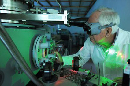 |
| Prof. Jerzy Wolowski from IPPLM near the new laser ion source.
|
|
Ion implementation is the process of embedding ions into the surface layer of the sample in order to change some properties of the material, mechanical or electrical. Currently, ion accelerators are routinely used for this purpose. Laser ion sources have a chance to excel those devices: they are smaller, simpler and can produce ions from high-melting materials such as tantalum or tungsten. What is more, the ion beam can easily be modified by the change of parameters and the geometry of the laser-target–sample system. The released ions can well be accelerated in the external electric field.
|
|
However, to be able to use the LIS type sources in industry, some requirements must be fulfilled: the beam of ions cannot possess impurities and the ions should have almost the same specific energy. To meet both requirements the laser ion source with special electrostatic system must be applied.
|
|
In the device built at the IPPLM the low-energy laser pulse lasts 3.5 nanoseconds. The laser pulse energy, in the first phase of laser-matter interaction, is transferred to free electrons which subsequently ionise atoms of target material and admixtures. The main part of the laser pulse energy directly heats ionised matter (plasma) causing its quick expansion. A broad energy distribution of the ions expanding from plasma results from the nature of the process of plasma generation.
|
|
Some particles and debris extracted from the target by the laser pulse are electrically neutral, which is why they expand without deflection in the electric field and go straight onto the screen that is placed exactly on the axis of the system, to shield the sample. At the same time, laser-produced ions which avoid the screen are accelerated and focused by the electric field on the sample located on the axis behind the screen. "We have selected the parameters of the field in such a way that only the chosen ions of the target reach the sample. The spot of the focused beam is 1 mm in diameter", explains Rosinski.
|
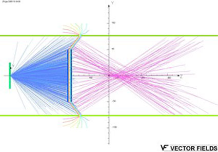 |
| Simulation of the trajectory of ions in laser ion source.
|
|
The low-energy laser used in the experiment does not heat itself and is capable of generating 10 thousand or more laser pulses within some ten minutes. Those advantages make it possible for scientists to control precisely the number of ions that reach the sample.
|
|
The solution proposed by the scientists from the IPPLM has successfully been used to explore the process of germanium ion implantation in silica (SiO2) layer with a view to fabricate germanium nanocrystals within it. Thus, a modified semiconductor has been created whose prospective implementation in electronics is widely anticipated, for example in miniaturisation of some memory chips or in elements for light emission.
|
|
To obtain germanium nanocrystals from the laser-produced ions, the implanted sample should be heated in the temperature of 600 to 1200 Celsius degrees. In this process some germanium crystals, ranging in size from a few to 20 nanometres (billionth of a metre) are created. "Our implanted samples, after heating, are examined with the use of various sophisticated, currently available measuring methods in the specialised laboratories, mainly at the Universities in Messina and Catania in Sicily. We have analysed both the results of ion implantation and the formation of nanocrystal structures in the samples", says Rosinski.
|
|
Laser ion source built and tested at the IPPLM is a prototype device expected to find applications in industry. "In two years, we will have finished the work connected with optimization of our device regarding industrial usage but we have already started looking for enterprises that are interested in implementing this technology", summarises Prof. Jerzy Wolowski, the Head of Laser Plasma Division at the IPPLM.
|
|
The construction of the device for laser induced implantation was started at the IPPLM a few years ago within the framework of European SEMINANO project. Nowadays, the Ministry of Science and Higher Education is the main source of financial support for this kind of research.
|