| Oct 31, 2011 |
Thin films: The electronic competition
|
|
(Nanowerk News) The atom-by-atom growth of a crystalline film on a crystalline substrate, a process known as epitaxy, is employed in a wide range of applications to produce high-performance electronic interfaces and functionalities. Achieving the highest-quality interfaces generally involves matching the atomic lattice structures of the film and substrate. However, depending on the pairing of materials, achieving such lattice matching can be difficult, and the mechanisms governing growth in lattice-mismatched systems can be complex.
|
|
Shu-Jung Tang and colleagues from National Tsing Hua University, the National Synchrotron Radiation Research Center and other institutions in Taiwan have now shown that the atomic structure of an epitaxial thin film is determined not only by atomic structural constraints, but also by electronic effects ("Electronic versus Lattice Match for Metal-Semiconductor Epitaxial Growth: Pb on Ge(111)").
|
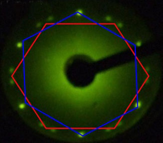 |
| Electron diffraction pattern for a four-monolayer-thick film of lead epitaxially grown on germanium. The two possible types of atomic order are indicated in blue (30° lattice-matched) and red (intrinsic lattice-mismatched).
|
|
The researchers investigated the epitaxial growth of lead on a germanium substrate. "Both materials have the same crystallographic structure in bulk, but their lattice constants are mismatched by 13%," explains Tang. This mismatch results in strain in the lead film if the two materials are aligned according to their intrinsic bulk orientations. However, an almost perfect lattice match between the two materials occurs if the atomic planes are rotated relative to each other by 30°.
|
|
To examine whether the lead films would adopt the lattice-matched configuration, Tang and his colleagues analyzed the atomic structures of a series of atomic monolayers of lead grown on germanium. They found that for very thin films, the lead atoms arrange themselves not in the lattice-matched orientation, but in the lattice-mismatched configuration (see image).
|
|
Further measurements revealed that the preference for the lattice-mismatched configuration stems from a strong electronic match between the two materials in this orientation — contrasted by an electronic mismatch in the lattice-matched configuration. Electronic matching, or the hybridization of electron wavefunctions at the interface, therefore appears to be a competing mechanism for producing a minimum-energy growth structure. As the film thickness is increased and electronic hybridization becomes weaker, the 30° lattice-matched domains begin to appear and eventually dominate film growth.
|
|
"Our results show that epitaxial growth is not solely determined by lattice match as traditionally thought, and are relevant for all thin-film systems that have strong electronic hybridization with their substrates," says Tang.
|