| Dec 05, 2011 |
Magnetoresistance: Silicon joins the party
|
|
(Nanowerk News) Giant magnetoresistance, which allows electrical resistance to be varied by relatively small magnetic fields, has had a huge impact on everyday technology, with widespread use in information storage and magnetic field sensing. Xiaozhong Zhang and colleagues from Tsinghua University in China have now demonstrated that it is possible to enhance inhomogeneous magnetoresistance (IMR) in silicon devices to levels comparable to that of conventional rare-earth-based technologies ("Geometrical enhancement of low-field magnetoresistance in silicon").
|
|
Most magnetoresistance-based devices are made from rare earth materials, which are expensive and in limited supply. The use of semiconductors like silicon as magnetoresistive components would not only lower costs but also allow ready integration with existing semiconductor technology. Magnetoresistance has recently been observed in non-magnetic semiconductors like silicon, and has been mainly attributed to charge inhomogeneities.
|
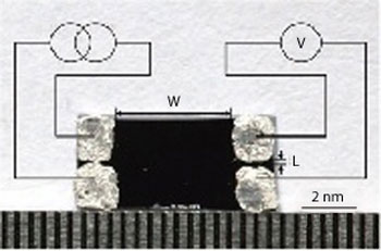 |
| Photograph of a silicon-based magnetoresistive element. (© 2011 Nature Publishing Group)
|
|
"Silcon-based IMR devices could be easily integrated into silicon chips," says Zhang. "They would endow present electronics with new operational modes based on the interplay between the electronics and the magnetic response, or magnetoelectronics."
|
|
The device developed by Zhang's team has a silicon active element and four indium electrodes for current injection and voltage drop measurements (see image). Injecting carriers can change the relative amount of electrons and holes and move the boundary between the two. When such a boundary is approximately in the middle of the device, the resistance reaches values close to 200% higher than usual and is very sensitive to small magnetic fields. As Zhang explains, the two factors could be combined to integrate low-field sensing and high-field sensing together in one device.
|
|
According to simulations, the IMR has two contributions: a difference in mobility between charges across the junction, and the role of the boundary in distorting the current path under a magnetic field. Most importantly, such distortion can be affected by the geometry of the contacts, and increases with the ratio between the width of the sample and the distance between the electrodes used to measure the voltage drop. This was verified by realizing a device with a width-to-length ratio of 120, which produced a magnetoresistance gain of up to 5,000%. Further optimization of the geometry is expected to increase the magnetoresistance even further, making silicon a promising alternative to rare earths for use in magnetoresistive devices.
|