| Jan 17, 2012 |
High-quality 64 kb ferroelectric NAND flash memory array
|
|
(Nanowerk News) Shigeki Sakai and others of Ferroelectric Memory Group, the Nanoelectronics Research Institute of the National Institute of Advanced Industrial Science and Technology (AIST), have developed a 64 kilobit (kb) memory cell array of a ferroelectric NAND (Fe-NAND) flash memory where each memory cell is a ferroelectric gate field effect transistor (FeFET), in collaboration with Ken Takeuchi (Associate Professor), Graduate School of Engineering, the University of Tokyo.
|
|
The first 64 kb Fe-NAND flash memory array with the all cells accessible has been produced by developing an FeFET circuit integration technology. The researchers also demonstrated the good data retention of the memory array by investigating a block (2 kb) of the memory cells for at least 2 days. The Fe-NAND flash memory is a potential next-generation nonvolatile semiconductor memory of high-density large-scale integration with a good endurance property and low power dissipation because it has the same cell-area scalability, about 1/7 as low power dissipation, and about 10000 times as many endurance cycles as the conventional NAND flash memory.
|
|
The details of this work were reported at the "2011 International Conference on Solid State Devices and Materials (SSDM 2011)", held in Nagoya.
|
|
Social Background of Research
|
|
Solid state drives (SSDs) have attracted much attention as small-and-lightweight mass storage devices which are replaceable for hard disk drives (HDDs) used in personal computers and server machines. Especially in data-center severs the SSDs are required to be introduced as a good solution to the recent increases of power consumption and heat generation with a rapidly growing amount of information processed. However, a conventional NAND flash memory, the key device of the SSD, has program/erase endurance cycles of only 10000 times which is insufficient to be used in the data-center severs for much data processing. The endurance of the NAND flash memory and the reliability of data will become worse when the memory cells proceed with downsizing for higher area densities. Therefore a next-generation nonvolatile semiconductor memory is expected which has good area-scalability and much more endurance cycles than the conventional NAND flash memory.
|
|
History of Research
|
|
AIST has been much experienced in the research on FeFETs which are interesting transistors with nonvolatile-memory function. In 2002, it succeeded in realizing long data retention of an FeFET for the first time by introducing a Pt/SrBi2Ta2O9/Hf-Al-O/Si gate stack. In 2004, AIST demonstrated the FeFET produced by a self-aligned-gate technique indicated a good area-scalability. In 2008, the researchers started a project for developing the Fe-NAND flash memory where the FeFETs are used as the memory cells, in collaboration with Prof. Takeuchi of the University of Tokyo. They demonstrated that the FeFETs can be used as the flash memory cells with good quality and scalability. The FeFETs had about 10000 times as many endurance cycles and about 1/3 as small program voltage as the conventional NAND flash memory cells. In the present work the researchers have succeeded in producing the first 64 kb Fe-NAND flash memory array with the all cells accessible by developing an FeFET circuit-integration technology. They also succeeded in demonstrating the good data retention of the flash memory array by investigating a block (2 kb) of the memory cells for at least 2 days.
|
|
This work was supported by New Energy and Industrial Technology Development Organization (NEDO) and was conducted as part of the NEDO project "Research of basic technology for developing novel ferroelectric flash memory (FY2009-FY2011)".
|
|
Details of Research
|
|
Figure 1 shows the 64 kb Fe-NAND flash memory array developed in this study. First a Si substrate designed for the Fe-NAND circuit was prepared by ion implantation. Then two layers were deposited on the Si which were about 7 nm-thick high-k Hf-Al-O (HAO) and about 500 nm-thick ferroelectric SrBi2Ta2O9 (SBT) by a large-area pulsed-laser deposition method. About 220 nm-thick metal Pt layer was deposited on the SBT layer. The gate electrodes and the contact holes were formed by photo-lithography. The Fe-NAND circuit was wired by two metal layers (M1 and M2) with an insulator layer between them. An Fe-NAND memory cell was an n-channel FeFET with a metal/ferroelectric/insulator/semiconductor stacked gate structure, namely Pt/SBT/HAO/Si. Both the gate length (L) and the gate width (W) were 5 ?m. The 64 kb Fe-NAND flash memory array was constructed by integrating 64 k memory cells of 256 by 256. A block selector and a bit-line selector on the two sides of the array were also constructed by n- and p-channel FeFETs designed in CMOS circuits. Totally 84 k FeFETs were used in the Fe-NAND flash memory array including the two selector circuits. A block out of all 32 blocks and a pair of neighboring bit-lines out of all 256 bit-lines were selectable at a time. Word-line voltages and bit-line voltages were applied from the outside pads in this work. Read-out of data was performed by measuring bit-line currents directly. The measurement system was made by a combination of pulse generators, DC current-and-voltage sources and semiconductor parameter analyzers. A computer was used for the automatic control of the system.
|
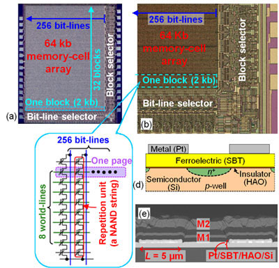 |
| Figure 1: The 64 kb Fe-NAND flash memory array developed in this study. Microscopic photos of (a) the whole chip and (b) an enlarged area around a corner. (c) Schematic circuits in a block. (d) Schematic drawing and (e) scanning-electron-microscopic photo of the cross section of the memory cell array.
|
|
The operation of block erase, page program, and data-nondestructive read were demonstrated by using the Fe-NAND flash memory array. The all 64 kb memory cells were accessible. The researchers succeeded in reading after programming the array in three patterns: all-bit-erase, all-bit-program, and checkerboard-program patterns. Figure 2 shows a result of reading after the all-bit-erase and the all-bit-program of the 64 kb memory cells. Good mass data-retention characteristics of a block (2 kb) were confirmed by at least 2 day-long measurements after the erase and after the program of each cell (Fig. 3). Good endurance characteristics of at least 108 erase-and-program cycles were also confirmed by a test memory cell on the same chip.
|
|
Figures 2 and 3 were made after inferior-bit counts were eliminated from the additions, which were 29.6 % of the 64 kb in Fig. 2 and 19 % of the 2 kb in Fig. 3. The reason of the inferior bits was accidental failures in the fabrication process of the selector circuits because the inferior bits shared blocks and/or bit-lines.
|
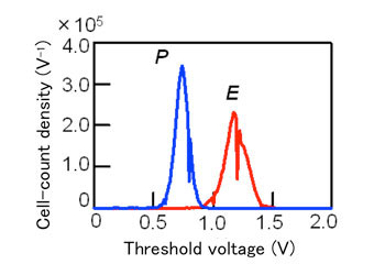 |
| Figure 2: Threshold-voltage distributions of all bits in the 64 kb Fe-NAND flash memory array. They were obtained by reading after the all-bit-erase (E) and after all-bit-program (P) of the 64 kb memory cells.
|
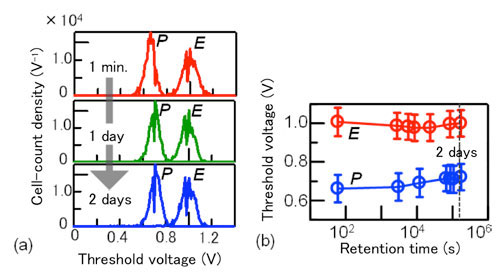 |
| Figure 3: (a) Threshold-voltage distributions of a block of memory cells investigated after 1 min., 1 day, and 2 days. (b) Mass data-retention characteristics by at least 2 day-long measurements. They were obtained by reading after the all-bit-erase. (E) and after all-bit-program (P) of the 2 kb memory cells.
|
|
The researchers have good prospects of lowering the bit-line voltages to 1 V and word-line voltages to 6 V at the data program. As a result, the Fe-NAND flash memory will have about 1/7 as small power consumption as the conventional NAND flash memory.
|
|
Future Plans
|
|
The researchers will proceed to downsize the Fe-NAND flash memory cells aiming at first L = 0.18 ?m, then L = 0.05 ?m, which are standard feature sizes of silicon devices, and finally they are aiming to achieve the industrial production in ten years. The first product will be a data-center SSD characterized by the very-low-power dissipation and high endurance over 108 cycles.
|